

Paper Menu >>
Journal Menu >>
 Modeling and Numerical Simulation of Material Science, 2013, 3, 4-8 Published Online January 2013 (http://www.SciRP.org/journal/mnsms) Copyright © 2013 SciRes. MNSMS Controllable Growth of Ni Nanocrystals Embedded in BaTiO3/SrTiO3 Superlattices Zhengwei Xiong, Weidong Wu Science and Technology on Plasma Physics Laboratory Research Center of Laser Fusion, China Academy of Engineering Physics Mianyan, China Email: [email protected] Received 2012 ABSTRACT BaT i O3/SrTiO3 superlattices with embedded Ni nanocrystals (NCs) have been grown on SrTiO3 (001) substrate using laser molecular beam epitaxy (L-MBE). In situ reflection high-energy electron diffraction (RHEED) was employed to investigate the process of lattice strain in the self-organization of Ni NCs and the epitaxial growth of BaTiO3/SrTiO3 superlattices. The results indicated that the strain from large lattice mismatch drove the self-organization of Ni NCs. Als o , the layer-by-layer growth of BaTiO3 /SrTiO3 superlattices and the island growth of Ni NCs were controllable ac- curately. The fine alternation of the two processes would provide a possible route to engineer controllably the nano- composite microstructure. Keywords: Nanocrystal; Superlattices; Self-organization 1. Introduction Oxide artificial superlattices, especially (001) oriented BaT i O3/SrTiO3 superlattices (BTO/STO SLs), have been attracted more attention because their dielectricand fer- roelectric properties can be enhanced by controlling the lattice strain along the polarized direction [1-3]. The di- electric matrix with the embedded metal NCs has widely potential application in nonlinear optical and electronic device [4, 5]. Therefore, several methods have been con- sidered to fabricate the BTO and STO-based material, including sol-gel [6], reactive evaporation [7], rf-sputtering [8] and laser ablation methods [9]. However, the controllable fabrication of nanostructure remains the daunting challenge for many deposition methods. There is an excellent method referred to as self-or ga nized growt h, in which the strain would drive the three -dimensional (3D) island to form in the lattice mis- matched growth process [10, 11]. Especially for the fa- brication of quantum dot (QD) structures, the self-or ga nized g rowth is greatly succe ss ful in semicon- ductor devices, such as InGaAs on GaAs [10], AlN on GaN [12]. Wu et al. have successfully fabricated Co:BTO and Ni:BTO composite film using self-organized method [13-15]. In this paper, the laser molecular beam epitaxy was used to embed the Ni NCs in the epitaxial films of Ba- TiO3/SrTiO3 superlattices (Ni NCs:BTO/STO SLs). The fabrication of the nanocomposite system is interesting and significant for both fundamental and application as- pects. Such composite films offer the combination of ferroelectric and ferromagnetic characteristics. This magnetoelectric interaction will be particularly strong in systems which simultaneously exhibit both ferromagnet- ism and ferroelectricity, i.e., in magnetoelectric multi- ferroics [16-18]. 2. Experimental The Ni NCs:BTO/STO SLs films were grown on STO (001) substrate with STO buffer layer by L-MBE. The acceleration voltage of RHEED electron gun was 25kev and the grazing incidence angle was about 1-3°. The growth process was performed in an ultrahigh -vac uu m (UHV) system and the background vacuum was ~2 ×10⁻⁶ Pa. The schematic diagram of Ni NCs:BTO/STO SLs film was shown in Fig. 1. The experimental parame- ters were listed in detail in Table 1. Before the deposition, the substrate STO (001) wa s in situ annealed about 2 hours in order to remove surface contamination. At 10 Pa oxygen pressure, the sample was annealed about 20 mi- nutes after accomplishing the BTO layer. The samples wer e characterized by XRD with Cu ka radiation and high -resolution transmission electron microscopy (HRTEM). 3. Results and discussion Fig.2 sho ws the oscillation of the RHEED intensity and 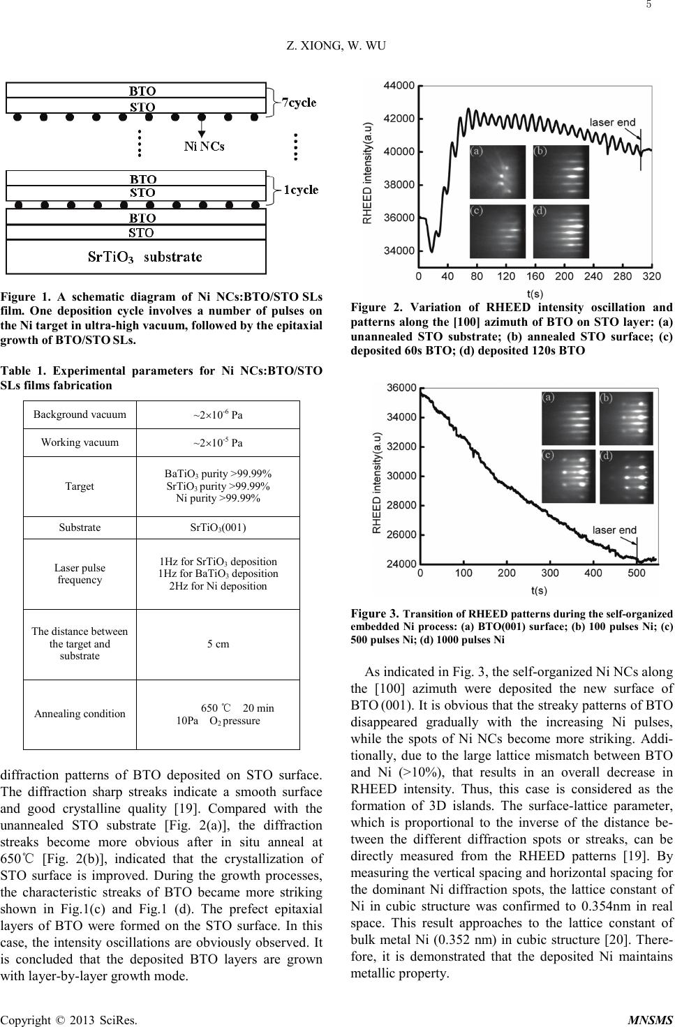 Z. XIONG, W. WU Copyright © 2013 SciRes. MNSMS Figure 1. A schematic diagram of Ni NCs:BTO/STO SLs film. One deposition cycle involves a number of pulses on the Ni target in ultra-high vacuum, followed by the epitaxial growth of BTO/STO SLs. Table 1. Experimental parameters for Ni NCs:BTO/STO SLs films fabrication Background vacuum ~2×10⁻⁶ Pa Working vacuum ~2×10⁻⁵ Pa Target BaTiO3 purity >99.99% SrTiO3 purity >99.99% Ni purity >99.99% Substrate SrTiO3(001) Laser pulse frequency 1Hz for SrTiO3 dep os i tion 1Hz for BaTiO3 dep os ition 2Hz for Ni deposition The distance between the target and substrate 5 cm Annealing condition 650 ℃ 20 min 10Pa O2 press u re diffraction patterns of BTO deposited on STO surface. The diffraction sharp streaks indicate a smooth surface and good crystalline quality [19]. Compared with the unannealed STO substrate [Fig. 2(a)], the diffraction streaks become more obvious after in situ anneal at 650℃ [Fig. 2(b)], indicated that the crystallization of STO surface is improved. During the growth processes, the characteristic streaks of BTO became more striking shown in Fig.1(c) and Fig.1 (d). The prefect epitaxial layers of BTO were formed on the STO s urface. In this case, the intensity oscillations are obviously observed. It is concluded that the deposited BTO layers are grown with la yer -by-layer growth mode. Figure 2. Variation of RHEED intensity oscillation and patterns along the [100] azimuth of BTO on STO layer: (a) unannealed STO substrate; (b) annealed STO surface; (c) deposited 60s BTO; (d) deposited 120s BTO Figure 3. Transition of RHEED patterns during the self-organized embe dded Ni process: (a) BTO(001) surface; (b) 100 pulses Ni; (c) 500 pulses Ni; (d) 1000 pulses Ni As indicated in Fig. 3, the self-o rga nize d Ni NC s along the [100] azimuth were deposited the new surface of BTO (001). It is obvious that the streaky patterns of BTO disappeared gradual ly wit h the increasing Ni pulses, while the spots of Ni NCs become more striking. Addi- tionally, due to the large lattice mismatch between BTO and Ni (>10%), that results in an overall decrease in RHEED intensity. Thus, this case is considered as the formation of 3D islands. The surface-lattice parameter, which is proportional to the inverse of the distance be- tween the different diffraction spots or streaks, can be directly measured from the RHEED patterns [19]. By measuring the vertical spacing and horizontal spacing for the dominant Ni diffraction spots, the lattice constant of Ni in cubic structure was c onf ir med to 0.354nm in real space. This result approaches to the lattice constant of bulk metal Ni (0.352 nm) in cubic structure [20]. There- for e, it is demonstrated that the deposited Ni maintains metallic property. 5 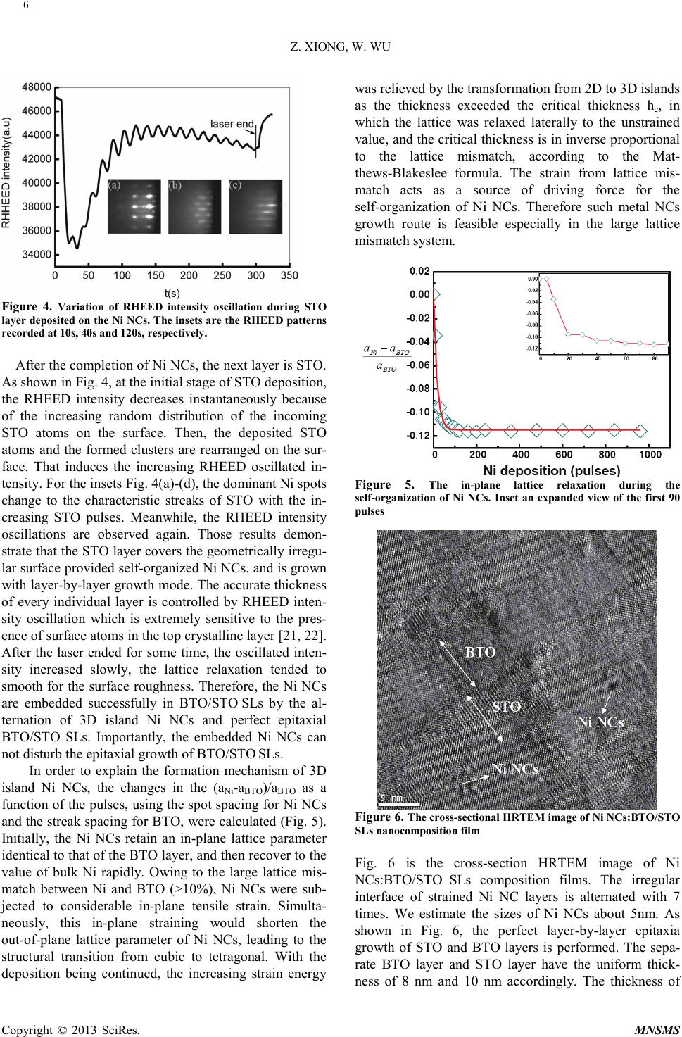 Z. XIONG, W. WU Copyright © 2013 SciRes. MNSMS Figure 4. Variation of RHEED intensity oscillation during STO layer deposited on the Ni NCs. The insets are the RHEED patterns recorded at 10s, 40s and 120s, respective ly. After the completion of Ni NCs, the next layer is STO. As shown in Fig. 4, at the initial stage of STO deposition, the RHEED intensity decreases instantaneously because of the increasing random distribution of the incoming STO atoms on the surface. Then, the deposited STO atoms and the formed clusters are rearranged on the sur- face. That induces the increasing RHEED oscillated in- tensity. For the insets Fig. 4(a)-(d), the dominant Ni spots change to the characteristic streaks of STO with the in- creasing STO pulses. Meanwhile, the RHEED intensity oscillations are observed again. Those results demon- strate that the STO layer covers the geometrically irregu- lar surface provided self-orga nize d Ni NCs, and is gro w n wit h layer-by-layer growth mode. The accurate thickness of every individual layer is controlled by RHEED inten- sity oscillation which is extremely sensitive to the pres- ence of surface atoms in the top crystalline layer [21, 22]. After the laser ended for some time, the oscillated inten- sity increased slowly, the lattice relaxation tended to smooth for the surface roughness. Therefore, the Ni NCs are embedded successfully in BTO/STO SLs by the al- ternation of 3D island Ni NCs and perfect epitaxial BTO/STO SLs. Importantly, the embedded Ni NCs can not disturb the epitaxial growth of BTO/STO SLs. In order to explain the formation mecha nis m of 3D island Ni NCs, the changes in the (aNi-aBTO)/aBTO as a function of the pulses, using the spot spacing for Ni NCs and the streak spacing for BTO, were calculated (Fig. 5). Initially, the Ni NCs retain an in-plane lattice parameter identical to that of the BTO layer, and then recover to the value of bulk Ni rapidly. Owing to the large lattice mis- match between Ni and BTO (>10%), Ni NCs were sub- jected to considerable in-plane tensile strain. Simulta- neously, this in-plane straining would shorten the out-of-plane lattice parameter of Ni NCs, leading to the structural transition from cubic to tetragonal. With the deposition being continued, the increasing strain energy was relieved by the transformation from 2D to 3D islands as the thickness exceeded the critical thickness hc, in which the lattice was relaxed laterally to the unstrained value, and the critical thickness is in inverse proportional to the lattice mismatch, according to the Mat- the ws -Blakeslee formula. The strain from lattice mis- match acts as a source of driving force for the self-organization of Ni NCs. Therefore such metal NCs growth route is feasible especially in the large lattice mismatch system. Figure 5. The in-plane lattice relaxation during the self-organization of Ni NCs. Inset an expanded view of the first 90 pulses Figure 6. The cross-sectional HRTEM image of Ni NCs:BTO/STO SLs nanocomposition film Fig. 6 is the cross-section HRTEM image of Ni NCs:BTO/STO SLs composition films. The irregular interface of strained Ni NC layers is alternated with 7 times. We estimate the sizes of Ni NCs about 5nm. As shown in Fig. 6, the perfect laye r-by-laye r epitaxia growth of STO and BTO layers is performed. The sepa- rate BTO layer and STO layer have the uniform thick- ness of 8 nm and 10 nm accordingly. The thickness of 6 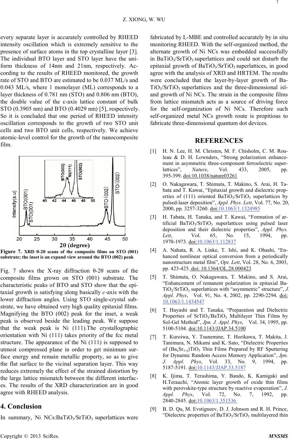 Z. XIONG, W. WU Copyright © 2013 SciRes. MNSMS every separate layer is accurately controlled by RHEED intensity oscillation which is extremely sensitive to the presence of surface atoms in the top crystalline layer [3]. The individual BTO layer and STO layer have the uni- form thickness of 14nm and 21nm, respectively. Ac- cording to the results of RHEED monitored, the growth rate of STO and BTO are estimated to be 0.037 ML/s and 0.043 ML/s, where 1 monolayer (ML) corresponds to a layer thickness of 0.781 nm (STO) and 0.806 nm (BTO), the double value of the c-axis lattice constant of bulk STO (0.3905 nm) and BTO (0.4029 nm) [5], respectively. So it is concluded that one period of RHEED intensity oscillation corresponds to the growth of two STO unit cells and two BTO unit cells, respectively. We achieve atomic-level control for the growth of the nanocomposite fil m. Figure 7. XRD θ-2θ scans of the composite films on STO (001) substrate; the inset is an expand view around the BTO (002) peak Fig. 7 shows the X-ray diffraction θ-2θ scans of the composite films grown on STO (001) substrate. The characteristic peaks of BTO and STO show that the epi- taxial growth is satisfying along basically c-axis with the lower diffraction angles. Using STO single-crystal sub- strate, we have obtained very high quality epitaxial films. Magnifying the BTO (002) peak for the inset, a weak peak is observed beside the leading peak. We suppose that the weak peak is Ni (111).The crystallographic orientation with Ni (111) takes priority of the fcc metal structure. The appearance of the Ni (111) is supposed to utmost compressed plane in order to get minimum sur- face energy and remain metallic property, so as to give the flat surface to the vicinal separation layer. This way reduces extremely the effect of the strained distortion by the large lattice mismatch between the different interfac- es. The results of the XRD characterization are in good agree with RHEED analysis. 4. Conclusion In summary, Ni NCs:BaTiO3/SrTiO3 superlattices were fabricated by L-MBE and controlled accurately by in situ monitoring RHEED. With the self-or ga nized method, the alternate growth of Ni NCs was embedded successfully in BaTiO3/SrTiO3 superlattices and could not disturb the epitaxial growth of BaTiO3/SrTiO3 superlattices, in good agree with the anal ysi s of XRD and HRTEM. The results wer e concluded that the layer-by-layer growth of Ba- TiO3/SrTiO3 superlattices and the t hree -dimensional isl- and growth of Ni NCs. The strain in the composite films from lattice mismatch acts as a source of driving force for the self-organization of Ni NCs. Therefore such self-or ga nized metal NCs growth route is propitious to fabricate three -di mensio nal quantum dot devices. REFERENCES [1] H. N. Lee, H. M. Christen, M. F. Chisholm, C. M. Rou- leau & D. H. Lownders, “Strong polarization enhance- ment in asymmetric three-component ferroelectric super- lattices”, Nature, Vol. 433, 2005, pp. 395-399. [2] O. Nakagawara, T. Shimuta, T. Makino, S. Arai, H. Ta- bata and T. Kawai, “Epitaxial growth and dielectric prop- erties of (111) oriented BaTiO3/SrTiO3 superlattices by pulsed-laser deposition”, Appl. Phys. Lett, Vol. 77, No. 20, 2000, pp. 3257-3260. doi: doi:10.1038/nature03261 10.1063/1.1324985 [3] H. Tabata, H. Tanaka, and T. Kawai, “Formation of ar- tificial BaTiO3/SrTiO3 superlattices using pulsed laser deposition and their dielectric properties”, Appl. Phys. Lett, Vol. 65, No. 15, 1994, pp. 1970-1973. [4] A. Nahata, R. A. Linke, T. Ishi, and K. Ohashi, “En- hanced nonlinear optical conversion from a periodically nanostructure metal film”, Opt. Lett, Vol. 28, No. 6, 2003, pp. 423-425. doi:10.1063/1.112837 [5] T. Shimuta, O. Nakagawara, T. Makino, and S. Arai, “Enhancement of remanent polarization in epitaxial Ba- TiO3/SrTiO3 superlattices with “asymmetric” structure”, J. Appl. Phys, Vol. 91, No. 4, 2002, pp. 2290-2294. doi: 10.1364/OL.28.000423 [6] T. Hayashi and T. Tanaka, “Preparation and Dielectric Properties of SrTiO3/BaTiO3 Multilayer Thin Films by Sol-Gel Method”, Jpn. J. Appl. Phys, Vol. 34, 1995, pp. 5100-5104. doi: 10.1063/1.1434547 [7] T. Kuroiwa, Y. Tsunemine, T. Horikawa, T. Makita, J. Tanimura, N. Mikami and K. Sato, “Dielectric Properties of (BaxSr1-x)TiO3 Thin Films Prepared by RF Sputtering for Dynamic Random Access Memory Application”, Jpn. J. Appl. Phys, Vol. 33, No. 9, 1994, pp. 5187-5191. doi:10.1143/JJAP.34.5100 [8] K. Ijima, T. Terashima, Y. Bando, K. Kamigaki and H.Terauch i, “Atomic layer growth of oxide thin films with perovskite-type structure by reactive evaporation”, J. Appl. Phys, Vol. 72, No. 7, 1992, pp. 2840-2845. doi:10.1143/JJAP.33.5187 [9] B. D. Qu, M. Evstigneev, D. J. Johnson and R. H. Prince, “Dielectric properties of BaTi O 3/SrTiO3 multilayered thin doi:10.1063/1.351536 7  Z. XIONG, W. WU Copyright © 2013 SciRes. MNSMS films prepared by pulsed laser deposition”, Appl. Phys. Lett, Vol. 72, No. 11, 1998, pp. 1394-1397. [10] H. Drexler, D. Leonard, W. Hansen, J. P. Kotthaus, and P. M.Petroff, “Spectroscopy of Quantum Levels in Charge-Tunable InGaAs Quantum Dots”, Phys. Rev. Lett, Vol. 73, No. 16, 1994, pp. 2252-2255. doi:1063/1.121066 [11] J. Coraux, V. Favre-Nicolin, H. Renevier, M. G. Proietti, B. Amstatt, E. Bellet-Amalric and B. Daudin, “Quantita- tive structural characterization of GaN quantum dot ripe- ningbusing reflection high-energy electron diffraction”, Appl. Phys. Lett, Vol. 101, No. 5, 2007, pp. 1-3. doi:10.1103/PhysRevLett.73.2252 [12] J. Coraux, H. Renevier, V. Favre-Nicolin, G. Renaud, and B. Daudin, “In situ resonant x-ray study of vertical corre- lation and capping effects during GaN/AlN quantum dot growth”, J. Appl. Phys, Vol. 88, No. 15, 2007, pp.1-3. doi: 10.1063/1.2422902 [13] W. Wu, Y. He, F. Wang, Z. Chen, Y. Tang and W. Sun, “Preparation and characterization of Co-BaTiO3 na- no-composite films by the pulsed laser deposition”, J. Crystal Growth, Vol. 289, No. 1, 2006, pp. 408-413. doi: 10.1063/1.2192572 [14] F. F. Ge, X. M. Wang, L. H. Cao, et al., “Self-Organized Ni Nanocrystal Embedded in BaTiO3 Epitaxial Film”, Nano Res. Lett, Vol. 5, No. 5, 2010, pp. 834-838. doi: 10.1016/j.jcrysgro.2005.11.041 [15] Z. Xiong, W. Sun, X. Wang, F. Jiang, W.Wu, “Dielectric enhancement of BaTiO 3/SrTiO3 superlattices with em- bedded Ni nanocrystals”, J. Alloys Compd, Vol. 513, 2012, pp. 300-303. doi: 10.1007/s11671-010-9570-9 [16] Y. H. Lin, S. Zhang, C. Deng, Y. Zhang, X. Wang, C. W. Nan, “Magnetic behavior and thickness dependence in Co-doped BaTiO3 thin films”, Appl. Phys. Lett, Vol. 92, No. 11, 2008, pp. 1-3. doi: 10.1016/j.jallcom.2011.09.103 [17] Y. H. Lin, J. Yuan, S. Zhang, et al., “Multiferroic beha- vior observed in highly orientated Mn-doped BaTi O 3 thin films”, Appl. Phys. Lett, Vol. 96, No. 3, 2009, pp. 1-3. doi:10.1063/1.2898525 [18] S. Geprägs, A. Brandlmaier, M. Opel, R. Gross, and S. T. B. Goennenwein, “Electric field controlled manipulation of the magnetization in Ni/BaTiO3 hybrid structures”, Appl. Phys. Lett, Vol. 96, No. 14, 2010, pp. 1-3. doi: 10.1063/1.3182793 [19] K. Godo, J. H. Chang, H. Makino, T. Takai, T. Hanada and T. Yao, T, Sascao, and T. Goto, “Formation processes of CdTe quantum dots on ZnTe substrates stu- died by reflection high-energy electron diffraction and photoluminescence”, J. Appl. Phys, Vol. 92, No. 9, 2002, pp. 5490-5493. doi: 10.1063/1.3377923 [20] S. M. Foiles, M. I. Baskes, and M. S. Daw, “Embed- ded-atom-method functions for the fcc metals Cu, Ag, Au, Ni, Pd, Pt, and their alloys”, Phys. Rev. B, Vol. 33, No. 12, 1986, pp. 7983-7991. doi: 10.1063/1.1513888 [21] B. Shin and M. J. Aziz, “Modeling RHEED intensity oscillations in multilayer epitaxy: Determination of the Ehrlich-Schwoebel barrier in Ge(001) homoepitaxy”, Phys. Rev. B, Vol. 76, No. 16, 2007, pp. 1-12. doi: 10.1103/PhysRevB.33.7983 [22] M. Dabrowska-Szata, “Analysis of RHEED pattern from semiconductor surfaces”, Mater. Chem Phys, Vol. 81, No. 2, 2003, pp. 257-259. doi: 10.1103/PhysRevB.76.165408 doi: 10.1016/S0254-0584(02)00569-2 8 |