

Paper Menu >>
Journal Menu >>
 Crystal Structure Theory and Applications, 2012, 1, 62-67 http://dx.doi.org/10.4236/csta.2012.13012 Published Online December 2012 (http://www.SciRP.org/journal/csta) Low Temperature Growth of Hydrogenated Silicon Prepared by PECVD from Argon Diluted Silane Plasma Rachid Amrani1,2*, Pascale Abboud1, Larbi Chahed2, Yvan Cuminal1 1IES, UMR, Université Montpellier II, Place Eugène Bataillon, Montpellier, France 2LPCMME, Département de Physique, Université d’Oran ES-Sénia, Oran, Algérie Email: *[email protected], [email protected] Received October 7, 2012; revised November 14, 2012; accepted November 23, 2012 ABSTRACT In order to contribute to the understanding of the optoelectronics properties of hydrogenated nanocrystalline silicon thin films, a detailed study has been conducted. The samples were deposited by 13.56 MHz PECVD (Plasma-Enhanced Chemical Vapor Deposition) of silane argon mixture. The argon dilution of silane for all samples studied was 96% by volume. The substrate temperature was fixed at 200˚C. The influence of depositions parameters on optical proprieties of samples was studied by UV-Vis-NIR spectroscopy. The structural evolution was studied by Raman spectroscopy and X-ray diffraction (XRD). Intrinsic-layer samples depositions were made in this experiment in order to obtain the transi- tion from the amorphous to crystalline phase materials. The deposition pressure varied from 400 mTorr to 1400 mTorr and the rf power from 50 to 250 W. The structural evolution studies show that beyond 200 W, we observed an amor- phous-nanocrystalline transition, with an increase in crystalline fraction by increasing rf power and working pressure. Films near the amorphous to nanocrystalline transition region are grown at reasonably high deposition rates (~10 Å/s), which are highly desirable for the fabrication of cost effective devices. The deposition rate increases with increasing rf power and process pressure. Different crystalline fractions (21% to 95%) and crystallite size (6 - 16 nm) can be achieved by controlling the process pressure and rf power. These structural changes are well correlated to the variation of optical proprieties of the thin films. Keywords: Silicon; PECVD; Deposition Rate; Amorphous Nanocrystalline Transition; Argon; Low Temperature 1. Introduction For high quality solar cell applications, materials with high optical absorption, high carrier mobility and low fabrication cost are demanded. Crystalline silicon (C-Si), the most popular electronic material, has an indirect bandgap and, hence, poor optical absorption. On the other hand, hydrogenated amorphous silicon (a-Si:H) has high optical absorption, but it suffers from low carrier mobility, photo-induced degradation also named Stabler- Wronski effect [1,2] and, hence, poor optoelectronic properties. Recently, thin film hydrogenated nanocry- stalline silicon (nc-Si:H) deposited by Plasma Enhanced Chemical Vapor Deposition (PECVD) emerged as a ma- terial for large-area electronics applications [3-6]. The fabrication cost for nc-Si:H optoelectronic applications is expected to be low, since thin films of nc-Si:H can be deposited directly over large-area substrates using the same fabrication facilities well established for a-Si:H devices. Plasma deposited hydrogenated nanocrystalline silicon (nc-Si:H) offers the possibilities of high carrier mobility and stability against Staebler-Wronski effects [6-9]. An enhanced optical absorption has been observed in nanocrystalline silicon films [10,11]. The nanocrystalline can absorb the photons of weak energies whereas amor- phous silicon effectively absorbs the photons of high energies. The optical absorption of nc-Si:H is evidently highly dependent on the crystalline fraction. In contrast to the a-Si:H film, the nc-Si:H film shows an increased absorption below 1.8 eV and a reduced absorption above 2.0 eV. With decreasing crystallinity, the absorption co- efficient decreases at lower photon energies nearly up to 1.4 eV, and increases beyond 2.0 eV [12]. The absorption coefficient of nc-Si:H is almost an or- der of magnitude higher than that of c-Si. Thus, only ~2 μm thick layer is necessary for the nanocrystalline cell compared to the >100 μm thick wafer used for a c-Si cell. The plasma-enhanced chemical vapor deposition (PECVD) method from silane plasma is widely used to deposit the amorphous and nanocrystalline hydrogenated silicon Si:H [13,14]. The importance of the effects of the gas dilution on the kinetics of powder formation is im- *Corresponding author. C opyright © 2012 SciRes. CSTA 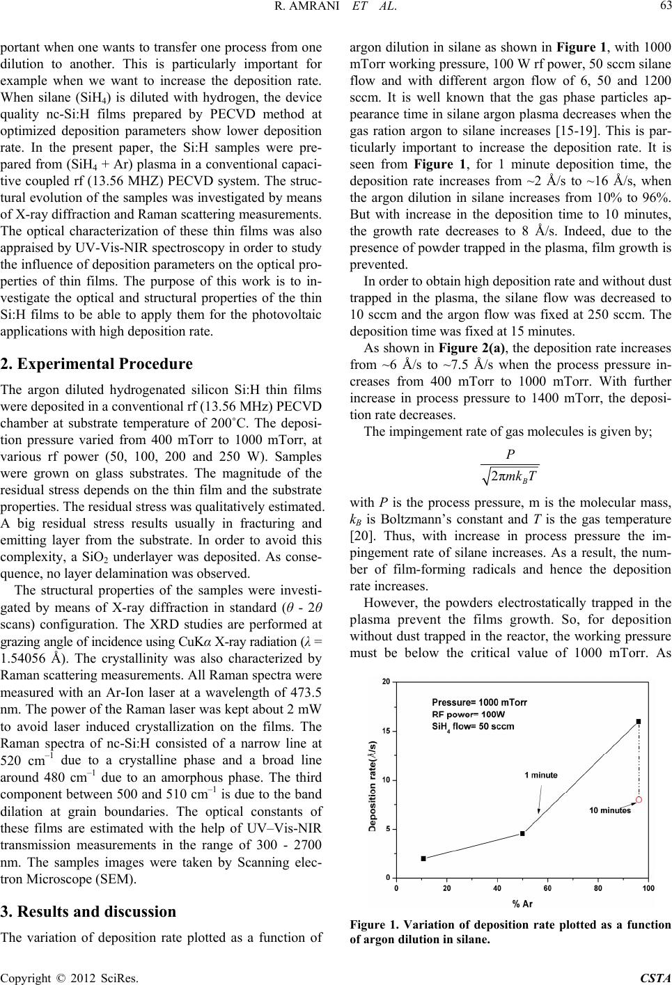 R. AMRANI ET AL. 63 portant when one wants to transfer one process from one dilution to another. This is particularly important for example when we want to increase the deposition rate. When silane (SiH4) is diluted with hydrogen, the device quality nc-Si:H films prepared by PECVD method at optimized deposition parameters show lower deposition rate. In the present paper, the Si:H samples were pre- pared from (SiH4 + Ar) plasma in a conventional capaci- tive coupled rf (13.56 MHZ) PECVD system. The struc- tural evolution of the samples was investigated by means of X-ray diffraction and Raman scattering measurements. The optical characterization of these thin films was also appraised by UV-Vis-NIR spectroscopy in order to study the influence of deposition parameters on the optical pro- perties of thin films. The purpose of this work is to in- vestigate the optical and structural properties of the thin Si:H films to be able to apply them for the photovoltaic applications with high deposition rate. 2. Experimental Procedure The argon diluted hydrogenated silicon Si:H thin films were deposited in a conventional rf (13.56 MHz) PECVD chamber at substrate temperature of 200˚C. The deposi- tion pressure varied from 400 mTorr to 1000 mTorr, at various rf power (50, 100, 200 and 250 W). Samples were grown on glass substrates. The magnitude of the residual stress depends on the thin film and the substrate properties. The residual stress was qualitatively estimated. A big residual stress results usually in fracturing and emitting layer from the substrate. In order to avoid this complexity, a SiO2 underlayer was deposited. As conse- quence, no layer delamination was observed. The structural properties of the samples were investi- gated by means of X-ray diffraction in standard (θ - 2θ scans) configuration. The XRD studies are performed at grazing angle of incidence using CuKα X-ray radiation (λ = 1.54056 Å). The crystallinity was also characterized by Raman scattering measurements. All Raman spectra were measured with an Ar-Ion laser at a wavelength of 473.5 nm. The power of the Raman laser was kept about 2 mW to avoid laser induced crystallization on the films. The Raman spectra of nc-Si:H consisted of a narrow line at 520 cm–1 due to a crystalline phase and a broad line around 480 cm–1 due to an amorphous phase. The third component between 500 and 510 cm–1 is due to the band dilation at grain boundaries. The optical constants of these films are estimated with the help of UV–Vis-NIR transmission measurements in the range of 300 - 2700 nm. The samples images were taken by Scanning elec- tron Microscope (SEM). 3. Results and discussion The variation of deposition rate plotted as a function of argon dilution in silane as shown in Figure 1, with 1000 mTorr working pressure, 100 W rf power, 50 sccm silane flow and with different argon flow of 6, 50 and 1200 sccm. It is well known that the gas phase particles ap- pearance time in silane argon plasma decreases when the gas ration argon to silane increases [15-19]. This is par- ticularly important to increase the deposition rate. It is seen from Figure 1, for 1 minute deposition time, the deposition rate increases from ~2 Å/s to ~16 Å/s, when the argon dilution in silane increases from 10% to 96%. But with increase in the deposition time to 10 minutes, the growth rate decreases to 8 Å/s. Indeed, due to the presence of powder trapped in the plasma, film growth is prevented. In order to obtain high deposition rate and without dust trapped in the plasma, the silane flow was decreased to 10 sccm and the argon flow was fixed at 250 sccm. The deposition time was fixed at 15 minutes. As shown in Figure 2(a), the deposition rate increases from ~6 Å/s to ~7.5 Å/s when the process pressure in- creases from 400 mTorr to 1000 mTorr. With further increase in process pressure to 1400 mTorr, the deposi- tion rate decreases. The impingement rate of gas molecules is given by; 2πB P mk T with P is the process pressure, m is the molecular mass, kB is Boltzmann’s constant and T is the gas temperature [20]. Thus, with increase in process pressure the im- pingement rate of silane increases. As a result, the num- ber of film-forming radicals and hence the deposition rate increases. However, the powders electrostatically trapped in the plasma prevent the films growth. So, for deposition without dust trapped in the reactor, the working pressure must be below the critical value of 1000 mTorr. As Figure 1. Variation of deposition rate plotted as a function of argon dilution in silane. Copyright © 2012 SciRes. CSTA 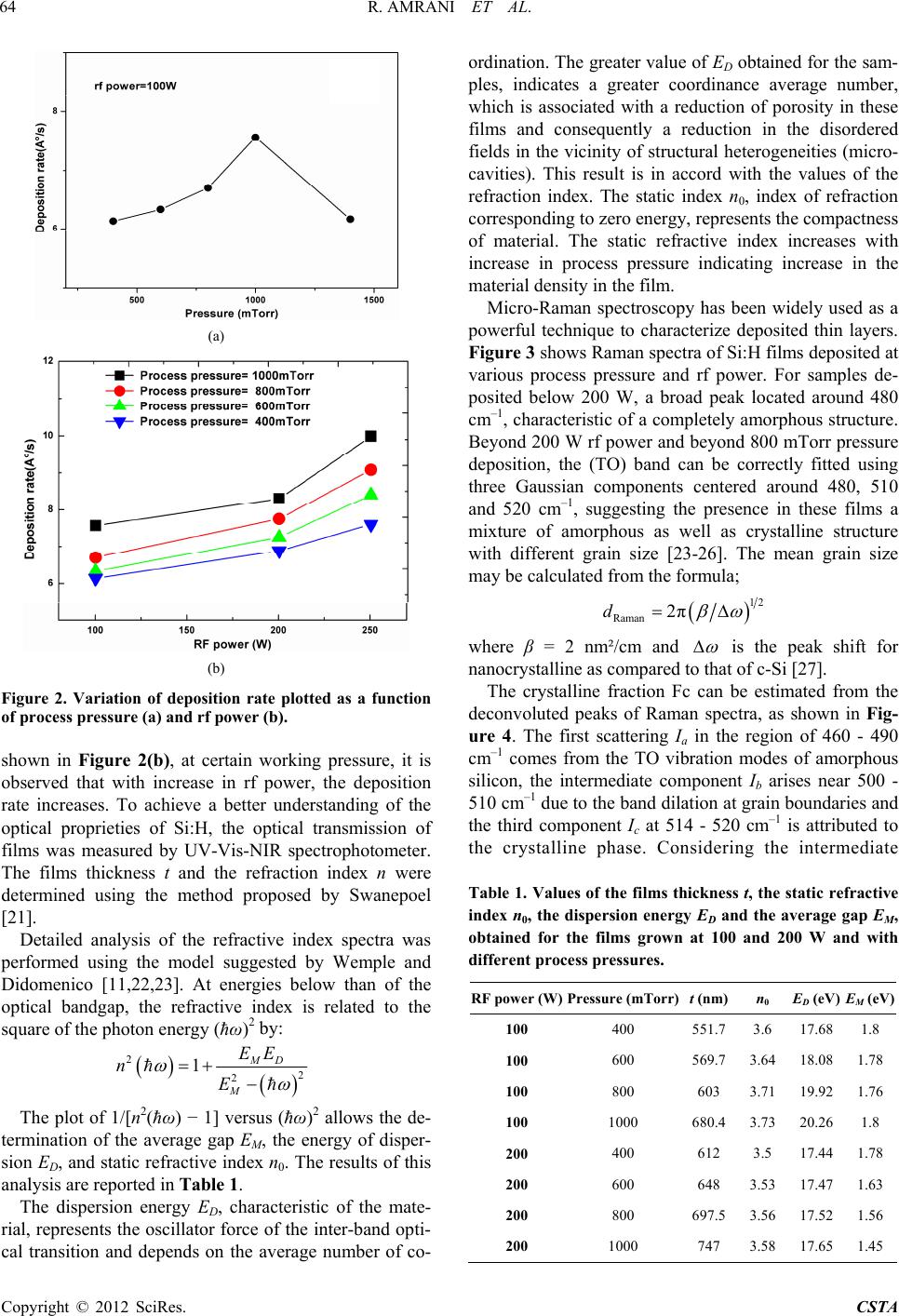 R. AMRANI ET AL. 64 (a) (b) Figure 2. Variation of deposition rate plotted as a function of process pressure (a) and rf power (b). shown in Figure 2(b), at certain working pressure, it is observed that with increase in rf power, the deposition rate increases. To achieve a better understanding of the optical proprieties of Si:H, the optical transmission of films was measured by UV-Vis-NIR spectrophotometer. The films thickness t and the refraction index n were determined using the method proposed by Swanepoel [21]. Detailed analysis of the refractive index spectra was performed using the model suggested by Wemple and Didomenico [11,22,23]. At energies below than of the optical bandgap, the refractive index is related to the square of the photon energy (ħω)2 by: 2 2 2 1 MD M EE n E The plot of 1/[n2(ħω) − 1] versus (ħω)2 allows the de- termination of the average gap EM, the energy of disper- sion ED, and static refractive index n0. The results of this analysis are reported in Table 1. The dispersion energy ED, characteristic of the mate- rial, represents the oscillator force of the inter-band opti- cal transition and depends on the average number of co- ordination. The greater value of ED obtained for the sam- ples, indicates a greater coordinance average number, which is associated with a reduction of porosity in these films and consequently a reduction in the disordered fields in the vicinity of structural heterogeneities (micro- cavities). This result is in accord with the values of the refraction index. The static index n0, index of refraction corresponding to zero energy, represents the compactness of material. The static refractive index increases with increase in process pressure indicating increase in the material density in the film. Micro-Raman spectroscopy has been widely used as a powerful technique to characterize deposited thin layers. Figure 3 shows Raman spectra of Si:H films deposited at various process pressure and rf power. For samples de- posited below 200 W, a broad peak located around 480 cm–1, characteristic of a completely amorphous structure. Beyond 200 W rf power and beyond 800 mTorr pressure deposition, the (TO) band can be correctly fitted using three Gaussian components centered around 480, 510 and 520 cm–1, suggesting the presence in these films a mixture of amorphous as well as crystalline structure with different grain size [23-26]. The mean grain size may be calculated from the formula; 12 Raman 2πd where β = 2 nm²/cm and is the peak shift for nanocrystalline as compared to that of c-Si [27]. The crystalline fraction Fc can be estimated from the deconvoluted peaks of Raman spectra, as shown in Fig- ure 4. The first scattering Ia in the region of 460 - 490 cm–1 comes from the TO vibration modes of amorphous silicon, the intermediate component Ib arises near 500 - 510 cm–1 due to the band dilation at grain boundaries and the third component Ic at 514 - 520 cm–1 is attributed to the crystalline phase. Considering the intermediate Table 1. Values of the films thickness t, the static refractive index n0, the dispersion energy ED and the average gap EM, obtained for the films grown at 100 and 200 W and with different process pressures. RF power (W)Pressure (mTorr) t (nm) n0 ED (eV) EM (eV) 100 400 551.7 3.6 17.681.8 100 600 569.7 3.64 18.081.78 100 800 603 3.71 19.921.76 100 1000 680.4 3.73 20.261.8 200 400 612 3.5 17.441.78 200 600 648 3.53 17.471.63 200 800 697.5 3.56 17.521.56 200 1000 747 3.58 17.651.45 Copyright © 2012 SciRes. CSTA 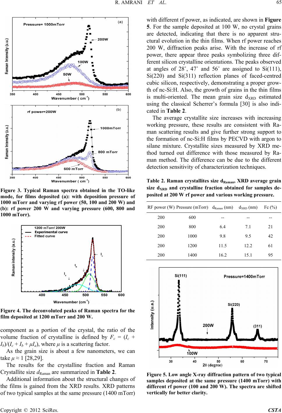 R. AMRANI ET AL. 65 Figure 3. Typical Raman spectra obtained in the TO-like mode, for films deposited (a): with deposition pressure of 1000 mTorr and varying rf power (50, 100 and 200 W) and (b): rf power 200 W and varying pressure (600, 800 and 1000 mTorr). Figure 4. The deconvoluted peaks of Raman spectra for the film deposited at 1200 mTorr and 200 W. component as a portion of the crystal, the ratio of the volume fraction of crystalline is defined by Fc = (Ic + Ib)/(Ic + Ib + μIa), where μ is a scattering factor. As the grain size is about a few nanometers, we can take μ ≈ 1 [28,29]. The results for the crystalline fraction and Raman Crystallite size dRaman are summarized in Table 2. Additional information about the structural changes of the films is gained from the XRD results. XRD patterns of two typical samples at the same pressure (1400 mTorr) with different rf power, as indicated, are shown in Figure 5. For the sample deposited at 100 W, no crystal grains are detected, indicating that there is no apparent stru- ctural evolution in the thin films. When rf power reaches 200 W, diffraction peaks arise. With the increase of rf power, there appear three peaks symbolizing three dif- ferent silicon crystalline orientations. The peaks observed at angles of 28˚, 47˚ and 56˚ are assigned to Si(111), Si(220) and Si(311) reflection planes of faced-centred cubic silicon, respectively, demonstrating a proper grow- th of nc-Si:H. Also, the growth of grains in the thin films is multi-oriented. The mean grain size dXRD estimated using the classical Scherrer’s formula [30] is also indi- cated in Table 2. The average crystallite size increases with increasing working pressure, these results are consistent with Ra- man scattering results and give further strong support to the formation of nc-Si:H films by PECVD with argon to silane mixture. Crystallite sizes measured by XRD me- thod turned out difference with those measured by Ra- man method. The difference can be due to the different detection sensitivity of characterization techniques. Table 2. Raman crystallites size dRaman, XRD average grain size dXRD and crystalline fraction obtained for samples de- posited at 200 W rf power and various working pressure. RF power (W)Pressure (mTorr)dRaman (nm) dXRD (nm)Fc (%) 200 600 -- -- -- 200 800 6.4 7.1 21 200 1000 9.8 9.5 42 200 1200 11.5 12.2 61 200 1400 16.2 15.1 95 Figure 5. Low angle X-ray diffraction pattern of two typical samples deposited at the same pressure (1400 mTorr) with different rf power (100 and 200 W). The spectra are shifted vertically for better clarity. Copyright © 2012 SciRes. CSTA 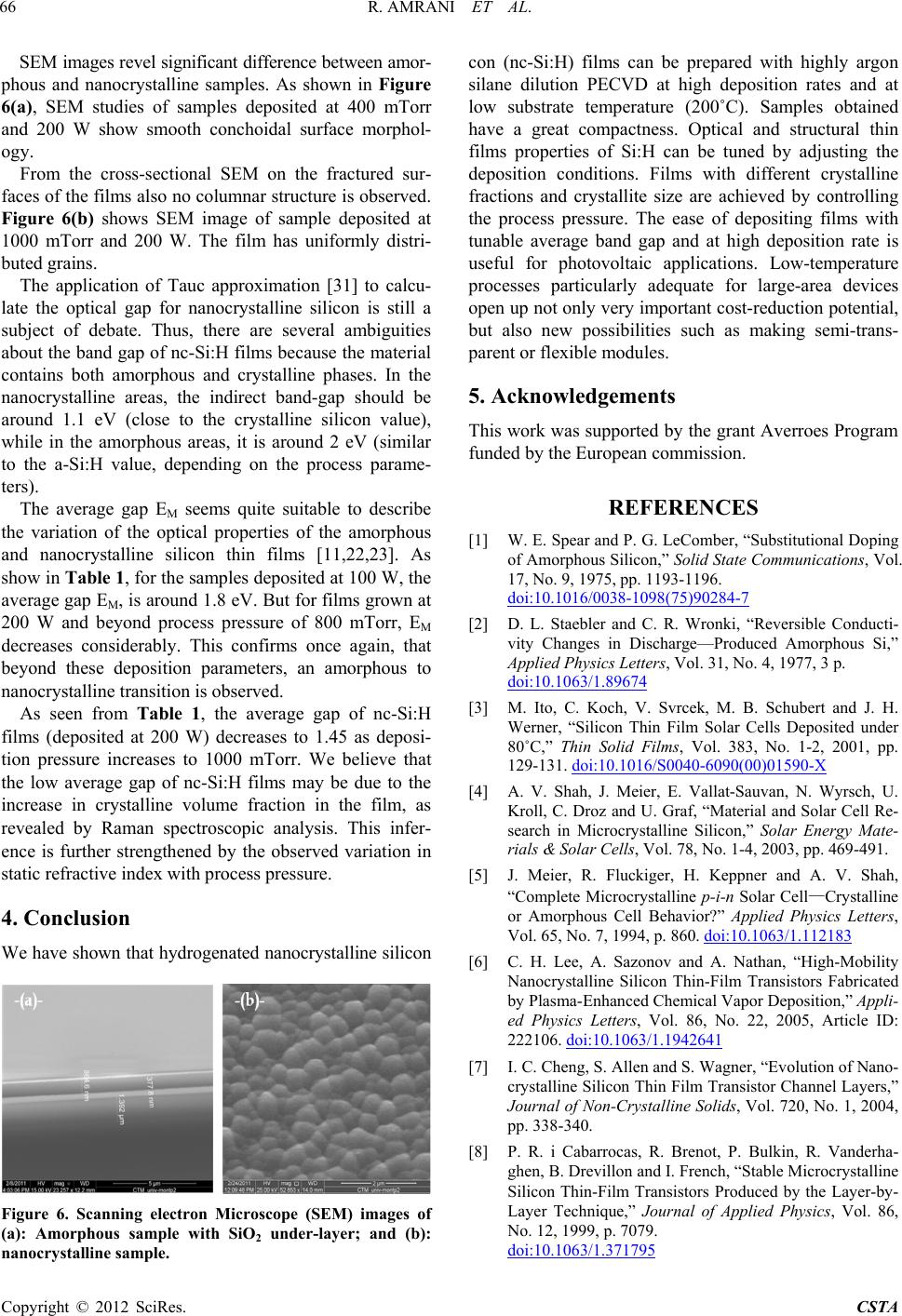 R. AMRANI ET AL. 66 SEM images revel significant difference between amor- phous and nanocrystalline samples. As shown in Figure 6(a), SEM studies of samples deposited at 400 mTorr and 200 W show smooth conchoidal surface morphol- ogy. From the cross-sectional SEM on the fractured sur- faces of the films also no columnar structure is observed. Figure 6(b) shows SEM image of sample deposited at 1000 mTorr and 200 W. The film has uniformly distri- buted grains. The application of Tauc approximation [31] to calcu- late the optical gap for nanocrystalline silicon is still a subject of debate. Thus, there are several ambiguities about the band gap of nc-Si:H films because the material contains both amorphous and crystalline phases. In the nanocrystalline areas, the indirect band-gap should be around 1.1 eV (close to the crystalline silicon value), while in the amorphous areas, it is around 2 eV (similar to the a-Si:H value, depending on the process parame- ters). The average gap EM seems quite suitable to describe the variation of the optical properties of the amorphous and nanocrystalline silicon thin films [11,22,23]. As show in Table 1, for the samples deposited at 100 W, the average gap EM, is around 1.8 eV. But for films grown at 200 W and beyond process pressure of 800 mTorr, EM decreases considerably. This confirms once again, that beyond these deposition parameters, an amorphous to nanocrystalline transition is observed. As seen from Table 1, the average gap of nc-Si:H films (deposited at 200 W) decreases to 1.45 as deposi- tion pressure increases to 1000 mTorr. We believe that the low average gap of nc-Si:H films may be due to the increase in crystalline volume fraction in the film, as revealed by Raman spectroscopic analysis. This infer- ence is further strengthened by the observed variation in static refractive index with process pressure. 4. Conclusion We have shown that hydrogenated nanocrystalline silicon Figure 6. Scanning electron Microscope (SEM) images of (a): Amorphous sample with SiO2 under-layer; and (b): nanocrystalline sample. con (nc-Si:H) films can be prepared with highly argon silane dilution PECVD at high deposition rates and at low substrate temperature (200˚C). Samples obtained have a great compactness. Optical and structural thin films properties of Si:H can be tuned by adjusting the deposition conditions. Films with different crystalline fractions and crystallite size are achieved by controlling the process pressure. The ease of depositing films with tunable average band gap and at high deposition rate is useful for photovoltaic applications. Low-temperature processes particularly adequate for large-area devices open up not only very important cost-reduction potential, but also new possibilities such as making semi-trans- parent or flexible modules. 5. Acknowledgements This work was supported by the grant Averroes Program funded by the European commission. REFERENCES [1] W. E. Spear and P. G. LeComber, “Substitutional Doping of Amorphous Silicon,” Solid State Communications, Vol. 17, No. 9, 1975, pp. 1193-1196. doi:10.1016/0038-1098(75)90284-7 [2] D. L. Staebler and C. R. Wronki, “Reversible Conducti- vity Changes in Discharge—Produced Amorphous Si,” Applied Physics Letters, Vol. 31, No. 4, 1977, 3 p. doi:10.1063/1.89674 [3] M. Ito, C. Koch, V. Svrcek, M. B. Schubert and J. H. Werner, “Silicon Thin Film Solar Cells Deposited under 80˚C,” Thin Solid Films, Vol. 383, No. 1-2, 2001, pp. 129-131. doi:10.1016/S0040-6090(00)01590-X [4] A. V. Shah, J. Meier, E. Vallat-Sauvan, N. Wyrsch, U. Kroll, C. Droz and U. Graf, “Material and Solar Cell Re- search in Microcrystalline Silicon,” Solar Energy Mate- rials & Solar Cells, Vol. 78, No. 1-4, 2003, pp. 469-491. [5] J. Meier, R. Fluckiger, H. Keppner and A. V. Shah, “Complete Microcrystalline p-i-n Solar Cell—Crystalline or Amorphous Cell Behavior?” Applied Physics Letters, Vol. 65, No. 7, 1994, p. 860. doi:10.1063/1.112183 [6] C. H. Lee, A. Sazonov and A. Nathan, “High-Mobility Nanocrystalline Silicon Thin-Film Transistors Fabricated by Plasma-Enhanced Chemical Vapor Deposition,” Appli- ed Physics Letters, Vol. 86, No. 22, 2005, Article ID: 222106. doi:10.1063/1.1942641 [7] I. C. Cheng, S. Allen and S. Wagner, “Evolution of Nano- crystalline Silicon Thin Film Transistor Channel Layers,” Journal of Non-Crystalline Solids, Vol. 720, No. 1, 2004, pp. 338-340. [8] P. R. i Cabarrocas, R. Brenot, P. Bulkin, R. Vanderha- ghen, B. Drevillon and I. French, “Stable Microcrystalline Silicon Thin-Film Transistors Produced by the Layer-by- Layer Technique,” Journal of Applied Physics, Vol. 86, No. 12, 1999, p. 7079. doi:10.1063/1.371795 Copyright © 2012 SciRes. CSTA  R. AMRANI ET AL. Copyright © 2012 SciRes. CSTA 67 [9] A. Shah, E. Vallat-Sauvain, P. Torres, J. Meier, U. Kroll, C. Hof, C. Droz, M. Goerlitzer, N. Wyrsch and M. Vane- cek, “Intrinsic Microcrystalline Silicon (μc-Si:H) Depos- ited by VHF-GD (Very High Frequency-Glow Discharge): A New Material for Photovoltaics and Optoelectronics,” Materials Science and Engineering: B, Vol. 69-70, 2000, pp. 219-226. doi:10.1016/S0921-5107(99)00299-8 [10] Z. Remes, “Study of Defects and Microstructure of Amor- phous and Microcrystalline Silicon Thin Films and Poly- crystalline Diamond Using Optical Methods,” Ph.D. The- sis, Charles University, Prague, 1999. [11] R. Amrani, D. Benlekehal, R. Baghdad, D. Senouci, A. Zeinert, K. Zellama, L. Chahed, J. D. Sib and Y. Bouizem, “Low-Temperature Growth of Nanocrystalline Silicon Films Prepared by RF Magnetron Sputtering: Structural and Optical Studies,” Journal of Non-Crystalline Solids, Vol. 354, No. 19-25, 2008, pp. 2291-2295. doi:10.1016/j.jnoncrysol.2007.10.044 [12] F. Siebke, S. Yata, Y. Hishikawa and M. Tanaka, “Cor- relation between Structure and Optoelectronic Properties of Undoped Microcrystalline Silicon,” Journal of Non- Crystalline Solids, Vol. 227-230, No. 2, 1998, pp. 977- 981. doi:10.1016/S0022-3093(98)00261-0 [13] A. Matsuda, “Thin-Film Silicon—Growth Process and Solar Cell Application,” Japanese Journal of Applied Physics, Vol. 43, 2004, pp. 7909-7920. doi:10.1143/JJAP.43.7909 [14] R. A. Street, “Large Area Electronics, Applications and Requirements,” Physica Status Solidi A, Vol. 166, No. 2, 1998, pp. 695-705. doi:10.1002/(SICI)1521-396X(199804)166:2<695::AID- PSSA695>3.0.CO;2-U [15] J. L. Dorier, C. Hollenstein and A. A. Howling, “Powder Dynamics in Very High Frequency Silane Plasmas,” Journal of Vacuum Science & Technology A, Vol. A10, No. 4, 1992, pp. 1048-1052. doi:10.1116/1.578200 [16] J. L. Dorier, C. Hollenstein and A. A. Howling, “Spatio- temporal Powder Formation and Trapping in Radio Fre- quency Silane Plasmas Using Two-Dimensional Polariza- tion—Sensitive Laser Scattering,” Journal of Vacuum Science & Technology A, Vol. 13, No. 3, 1995, pp. 918-928. doi:10.1116/1.579852 [17] A. A. Howling, J. L. Dorier, C. Hollenstein, U. Kroll and F. Finger, “Frequency Effects in Silane Plasmas for Plasma Enhanced Chemical Vapor Deposition,” Journal of Vacuum Science & Technology A, Vol. 10, No. 4, 1992, pp. 1080-1085. doi:10.1116/1.578205 [18] J. L. Dorier, “Genèse, Croissance et Conséquences de Particules Dans les Plasmas en Silane à Basse Pression et Basse Température,” Ph.D. Thesis, 1996. [19] A. Bouchoule, “Dusty Plasma: Physics, Chemistry and Technological Impacts in Plasma Processing,” Wiley, New York, 1999. [20] S. Kasap and P. Capper, “Springer Handbook of Elec- tronic and Photonic Materials,” Springer Publication, 2006. [21] R. Swanpoel, “Determination of the Thickness and Op- tical Constants of Amorphous Silicon,” Journal of Phy- sics E: Scientific Instruments, Vol. 16, No. 12, 1983, pp. 1214-1222. doi:10.1088/0022-3735/16/12/023 [22] S. H. Wemple and M. Didomenico, “Behavior of the Electronic Dielectric Constant in Covalent and Ionic Ma- terials,” Physical Review B, Vol. 3, No. 4, 1971, pp. 1338- 1351. doi:10.1103/PhysRevB.3.1338 [23] R. Amrani, F. Pichot, J. Podlecki, A. Foucaran, L. Chah- ed and Y. Cuminal, “Optical and Structural Proprieties of nc-Si:H Prepared by Argon Diluted Silane PECVD,” Journal of Non-Crystalline Solids, Vol. 358, No. 17, 2012, pp. 1978-1982. doi:10.1016/j.jnoncrysol.2012.01.022 [24] S. Veprek, F. A Sarott and Z. Iqbal, “Effect of Grain Boun- daries on the Raman Spectra, Optical Absorption, and Elastic Light Scattering in Nanometer-Sized Crystalline Silicon,” Physical Review B, Vol. 36, No. 6, 1987, p. 3444. [25] H. S. Mavi, A. K. Shukla, S. C. Abbi and K. P. Jain, “Raman Study of Amorphous to Microcrystalline Phase Transition in cw Laser Annealed a-Si:H Films,” Journal of Physic Science, Vol. 66, No. 11, 1989, p. 5322. doi:10.1063/1.343723 [26] Y. He, Y. Wei, G. Zheng, M. Yu and M. Liu, “An Ex- ploratory Study of the Conduction Mechanism of Hydro- genated Nanocrystalline Silicon Films,” Journal of Ap- plied Physics, Vol. 82, No. 7, 1997, p. 3408. doi:10.1063/1.365656 [27] Y. He, C. Yin, G. Cheng, L. Wang, X. Liu and G. H. Hu, “The Structure and Properties of Nanosize Crystalline Silicon Films,” Journal of Applied Physics, Vol. 75, No. 2, 1994, pp. 797-803. doi:10.1063/1.356432 [28] G. Yue, J. D. Lorentzien, J. Lin, D. Han and Q. Wang, “Photoluminescence and Raman Studies in Thin-Film Materials: Transition from Amorphous to Microcrystal- line Silicon,” Applied Physics Letters, Vol. 75, No. 4, 1988, pp. 492-494. doi:10.1063/1.124426 [29] D. Beeman, R. Tsu and M. F. Tporpe, “Structural Infor- mation from the Raman Spectrum of Amorphous Sili- con,” Physical Review B, Vol. 32, No. 2, 1985, pp. 874- 878. doi:10.1103/PhysRevB.32.874 [30] P. Scherrer, “Bestimmung der Grösse und Derinneren Struktur von Kolloidteilchen Mittels Röntgenstrahlen,” Nachrichten von der Gesellschaft der Wissenschaften zu Göttingen, Mathematisch-Physikalische Klasse, Vol. 26, No. 1, 1918, pp. 98-100. [31] J. Tauc, “Optical Properties of Solids,” Abeles, North Holland, Amsterdam, 1972. |