

Paper Menu >>
Journal Menu >>
 Optics and Photonics Journal, 2012, 2, 260-264 http://dx.doi.org/10.4236/opj.2012.24031 Published Online December 2012 (http://www.SciRP.org/journal/opj) Phase-Matching and Parametric Conversion for the Mid-Infrared in As2S3 Waveguides Qi Chen, Xin Wang, Christi Madsen Department of Electrical & Computer Engineering, Texas A&M University, College Station, USA Email: [email protected] Received September 7, 2012; revised October 5, 2012; accepted October 17, 2012 ABSTRACT We illustrate two As2S3 waveguide designs for four-wave mixing, which can generate 3.03 μm mid-infrared light from a 1.55 μm near-infrared signal source and a 2.05 μm pump source. Through simulations, we verify that four-wave mix- ing phase-matching efficiencies up to 100% can be achieved using dispersion engineering to maintain the dispersion at 2.05 μm near to zero. The best conversion efficiency is –10 dB. When the waveguide length is 1 cm, the parametric conversion bandwidth is 1525 nm. We also evaluated the shift of 100% phase-matching efficiency wavelengths based upon fabrication tolerances. Keywords: As2S3; Mid-Infrared; Phase-Matching; Four-Wave Mixing 1. Introduction Four-wave mixing (FWM) is a third-order nonlinear process. In degenerate FWM, if the phase-matching con- dition is met, two pump photons and a signal photon can generate an idler photon. In mid-infrared (Mid-IR) region, the vast majority of gaseous chemical substances exhibit fundamental vibrational absorption bands, and the ab- sorption of light provides a nearly universal means for their detection [1]. The high sensitivity and capability of non-intrusive in-situ detection make it ideal for trace gas detection. Recently, although many papers have been published on FWM in silicon waveguides for both near-infrared (near-IR) [2-9] and mid-IR [10,11] and in chalcogenide waveguides for near-IR [12-14], the parametric conver- sion by FWM for mid-IR in chalcogenide waveguides has not been demonstrated yet. In addition, the applica- tions silicon waveguides cannot be utilized over 2.5 μm wavelength region due to the strong absorption from the substrate material, silicon dioxide (SiO2). On the contrary, lithium niobate (LiNbO3), as a widely-used optical mate- rial, has very high transmission over the wavelength range from 0.42 to 5.2 μm and exhibits excellent electro- optic, nonlinear and piezoelectric properties. Therefore, it is a good substrate material for mid-IR integrated optics up to 5 μm. Chalcogenide glasses have been investigated as an al- ternative platform for nonlinear signal processing [15]. They are a set of amorphous materials which show good transparency and low loss for both 1.3 μm - 1.55 μm tele- communication windows and into the mid-IR region. Arsenic tri-sulfide (As2S3) is very popular among them by its low two photon absorption (TPA) coefficient, which makes it ideal for nonlinear optics. Magnesium fluoride (MgF2), which has wide transmission range (0.2 μm - 7 μm) into the mid-IR, is a good candidate for clad- ding material because of its lower refractive index. Magnesium fluoride (MgF2), which has wide transmis- sion range (0.2 μm - 7 μm) at mid-IR, is a good candidate for cladding material because of its ruggedness and dura- bility. It also keeps the potential of optical tuning by adding electrodes on it. In this paper, we report two As2S3 waveguide designs, which have near zero dispersion at a pump wavelength of 2.05 μm and satisfy the phase-matching condition at a signal wavelength of 1.55 μm. The corresponding idler wavelength is 3.03 μm which is a common operation wavelength for trace gas sensors [16]. The FWM phase- matching efficiency can be as high as 100%. Through simulations, we verify that the parametric conversion efficiency is –10 dB for pump power intensity of 0.1 GW/cm2. Under the same intensities, our results are 20 dB better than the parametric conversion efficiency of silicon waveguides. 2. Dispersion Engineering To satisfy the phase-matching condition, dispersion en- gineering is required. In the first place, we have to main- tain the very low dispersion at the pump wavelength by varying the waveguide dimensions. To achieve high effi- C opyright © 2012 SciRes. OPJ 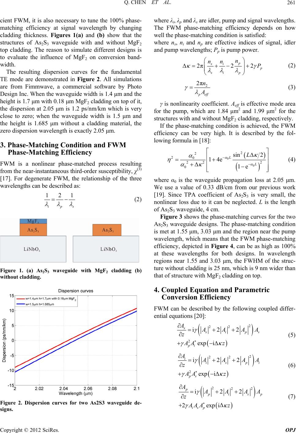 Q. CHEN ET AL. 261 cient FWM, it is also necessary to tune the 100% phase- matching efficiency at signal wavelength by changing cladding thickness. Figures 1(a) and (b) show that the structures of As2S3 waveguide with and without MgF2 top cladding. The reason to simulate different designs is to evaluate the influence of MgF2 on conversion band- width. The resulting dispersion curves for the fundamental TE mode are demonstrated in Figure 2. All simulations are from Fimmwave, a commercial software by Photo Design Inc. When the waveguide width is 1.4 μm and the height is 1.7 μm with 0.18 μm MgF2 cladding on top of it, the dispersion at 2.05 μm is 1.2 ps/nm/km which is very close to zero; when the waveguide width is 1.5 μm and the height is 1.685 μm without a cladding material, the zero dispersion wavelength is exactly 2.05 μm. 3. Phase-Matching Condition and FWM Phase-Matching Efficiency FWM is a nonlinear phase-matched process resulting from the near-instantaneous third-order susceptibility, χ(3) [17]. For degenerate FWM, the relationship of the three wavelengths can be described as: 121 ips (2) Figure 1. (a) As2S3 waveguide with MgF2 cladding (b) without cladding. Figure 2. Dispersion curves for two As2S3 waveguide de- signs. where λi, λp and λs are idler, pump and signal wavelengths. The FWM phase-matching efficiency depends on how well the phase-matching condition is satisfied: where ns, ni and np are effective indices of signal, idler and pump wavelengths; Pp is pump power. 2π22 p si p si p n nn P (2) 2 2π peff n A (3) γ is nonlinearity coefficient. Aeff is effective mode area for the pump, which are 1.84 μm2 and 1.99 μm2 for the structures with and without MgF2 cladding, respectively. If the phase-matching condition is achieved, the FWM efficiency can be very high. It is described by the fol- lowing formula in [18]: 0 0 2 2 20 22 2 0 sin 2 14e 1e L L L (4) where α0 is the waveguide propagation loss at 2.05 μm. We use a value of 0.33 dB/cm from our previous work [19]. Since TPA coefficient of As2S3 is very small, the nonlinear loss due to it can be neglected. L is the length of As2S3 waveguide, 4 cm. Figure 3 shows the phase-matching curves for the two As2S3 waveguide designs. The phase-matching condition is met at 1.55 μm, 3.03 μm and the region near the pump wavelength, which means that the FWM phase-matching efficiency, depicted in Figure 4, can be as high as 100% at these wavelengths for both designs. In wavelength regions near 1.55 and 3.03 μm, the FWHM of the struc- ture without cladding is 25 nm, which is 9 nm wider than that of structure with MgF2 cladding on top. 4. Coupled Equation and Parametric Conversion Efficiency FWM can be described by the following coupled differ- ential equations [20]: 2 22 2 i22 exp i s s ip pi A s A AA z AA z A (5) 2 22 2 i22 exp i i ispi ps A A AAA z AA z (6) 222 i22 2expi p p is isp A p A AA z AAA z A (7) Copyright © 2012 SciRes. OPJ 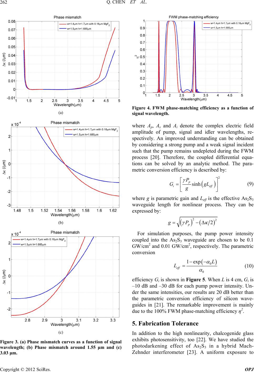 Q. CHEN ET AL. 262 (a) (b) (c) Figure 3. (a) Phase mismatch curves as a function of signal wavelength; (b) Phase mismatch around 1.55 μm and (c) 3.03 μm. Figure 4. FWM phase-matching efficiency as a function of signal wavelength. where Ap, As and Ai denote the complex electric field amplitude of pump, signal and idler wavelengths, re- spectively. An improved understanding can be obtained by considering a strong pump and a weak signal incident such that the pump remains undepleted during the FWM process [20]. Therefore, the coupled differential equa- tions can be solved by an analytic method. The para- metric conversion efficiency is described by: 2 sinh p i P Gg g e ff L (9) where g is parametric gain and Leff is the effective As2S3 waveguide length for nonlinear process. They can be expressed by: 22 2 p gP For simulation purposes, the pump power intensity coupled into the As2S3 waveguide are chosen to be 0.1 GW/cm2 and 0.01 GW/cm2, respectively. The parametric conversion 0 0 1exp eff L L (10) efficiency Gi is shown in Figure 5. When L is 4 cm, Gi is –10 dB and –30 dB for each pump power intensity. Un- der the same intensities, our results are 20 dB better than the parametric conversion efficiency of silicon wave- guides in [21]. The remarkable improvement is mainly due to the 100% FWM phase-matching efficiency η2. 5. Fabrication Tolerance In addition to the high nonlinearity, chalcogenide glass exhibits photosensitivity, too [22]. We have studied the photodarkening effect of As2S3 in a hybrid Mach- Zehnder interferometer [23]. A uniform exposure to Copyright © 2012 SciRes. OPJ 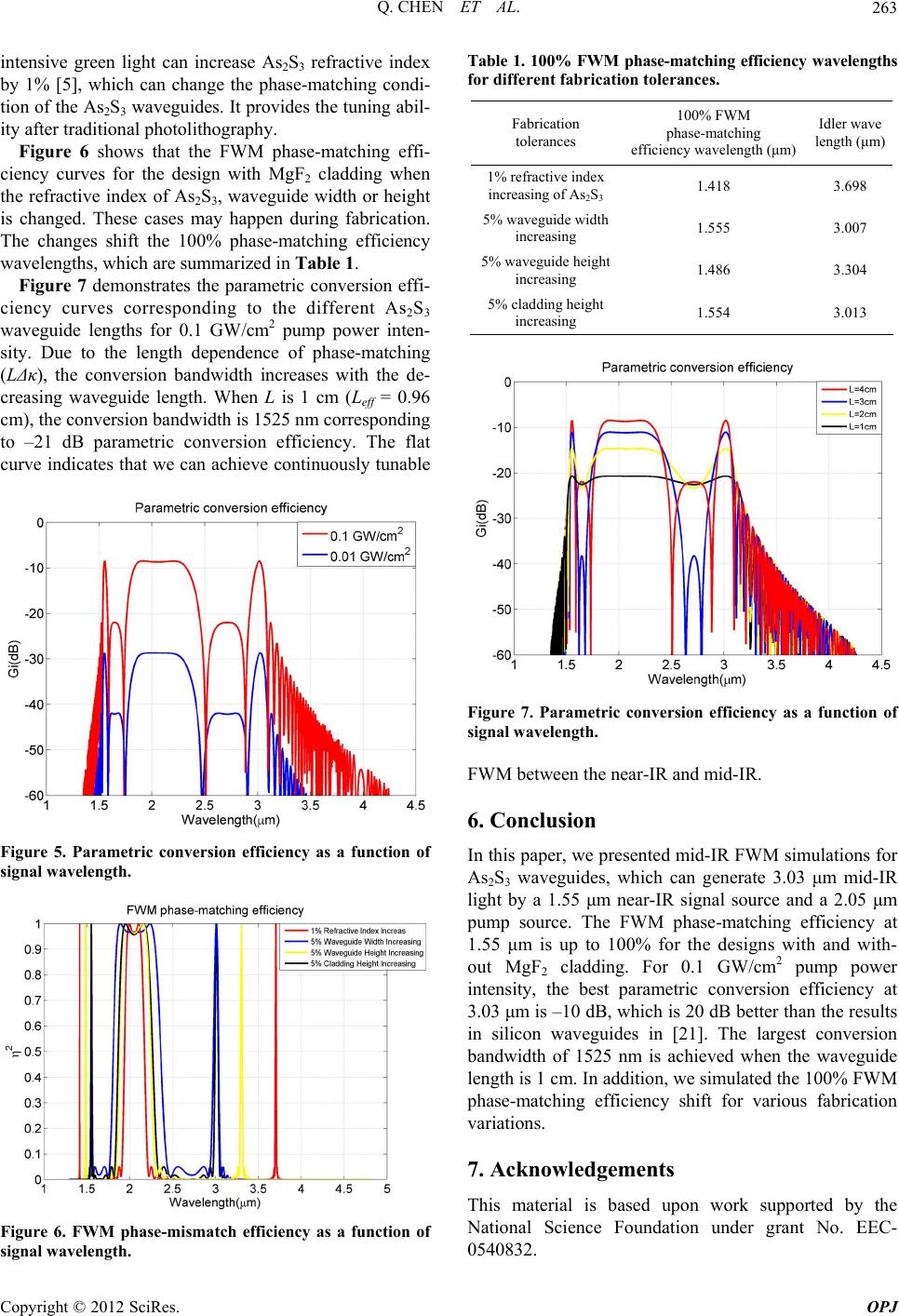 Q. CHEN ET AL. 263 intensive green light can increase As2S3 refractive index by 1% [5], which can change the phase-matching condi- tion of the As2S3 waveguides. It provides the tuning abil- ity after traditional photolithography. Figure 6 shows that the FWM phase-matching effi- ciency curves for the design with MgF2 cladding when the refractive index of As2S3, waveguide width or height is changed. These cases may happen during fabrication. The changes shift the 100% phase-matching efficiency wavelengths, which are summarized in Table 1. Figure 7 demonstrates the parametric conversion effi- ciency curves corresponding to the different As2S3 waveguide lengths for 0.1 GW/cm2 pump power inten- sity. Due to the length dependence of phase-matching (LΔκ), the conversion bandwidth increases with the de- creasing waveguide length. When L is 1 cm (Leff = 0.96 cm), the conversion bandwidth is 1525 nm corresponding to –21 dB parametric conversion efficiency. The flat curve indicates that we can achieve continuously tunable Figure 5. Parametric conversion efficiency as a function of signal wavelength. Figure 6. FWM phase-mismatch efficiency as a function of signal wavelength. Table 1. 100% FWM phase-matching efficiency wavelengths for different fabrication tolerances. Fabrication tolerances 100% FWM phase-matching efficiency wavelength (μm) Idler wave length (μm) 1% refractive index increasing of As2S3 1.418 3.698 5% waveguide width increasing 1.555 3.007 5% waveguide height increasing 1.486 3.304 5% cladding height increasing 1.554 3.013 Figure 7. Parametric conversion efficiency as a function of signal wavelength. FWM between the near-IR and mid-IR. 6. Conclusion In this paper, we presented mid-IR FWM simulations for As2S3 waveguides, which can generate 3.03 μm mid-IR light by a 1.55 μm near-IR signal source and a 2.05 μm pump source. The FWM phase-matching efficiency at 1.55 μm is up to 100% for the designs with and with- out MgF2 cladding. For 0.1 GW/cm2 pump power intensity, the best parametric conversion efficiency at 3.03 μm is –10 dB, which is 20 dB better than the results in silicon waveguides in [21]. The largest conversion bandwidth of 1525 nm is achieved when the waveguide length is 1 cm. In addition, we simulated the 100% FWM phase-matching efficiency shift for various fabrication variations. 7. Acknowledgements This material is based upon work supported by the National Science Foundation under grant No. EEC- 0540832. Copyright © 2012 SciRes. OPJ  Q. CHEN ET AL. Copyright © 2012 SciRes. OPJ 264 REFERENCES [1] F. Tittel, D. Richter and A. Fried, “Mid-Infrared Laser Applications in Spectroscopy,” Solid-State Mid-Infrared Laser Sources, 2003, pp. 458-529. [2] M. A. Foster, A. C. Turner, J. E. Sharping, B. S. Schmidt, M. Lipson and A. L. Gaeta, “Broad-Band Optical Para- metric Gain on a Silicon Photonic Chip,” Nature, Vol. 441, No. 7096, 2006, pp. 960-963. doi:10.1038/nature04932 [3] Q. Lin, J. D. Zhang, P. M. Fauchet and G. P. Agrawal, “Ultrabroadband Parametric Generation and Wavelength Conversion in Silicon Waveguides,” Optics Express, Vol. 14, No. 11, 2006, pp. 4786-4799. doi:10.1364/OE.14.004786 [4] A. C. Turner, C. Manolatou, B. S. Schmidt, M. Lipson, M. A. Foster, J. E. Sharping and A. L. Gaeta, “Tailored Anomalous Group-Velocity Dispersion in Silicon Chan- nel Waveguides,” Optics Express, Vol. 14, No. 10, 2006, pp. 4357-4362. doi:10.1364/OE.14.004357 [5] D. Dimitropoulos, V. Raghunathan, R. Claps and B. Jalali, “Phase-Matching and Nonlinear Optical Processes in Sili- con Waveguides,” Optics Express, Vol. 12, No. 1, 2004, pp. 149-160. http://www.opticsinfobase.org/abstract.cfm?URI=oe-12-1 -149 doi:10.1364/OPEX.12.000149 [6] V. Raghunathan, R. Claps, D. Dimitropoulos and B. Jalali, “Parametric Raman Wavelength Conversion in Scaled Silicon Waveguides,” Journal of Lightwave Technology, Vol. 23, No. 6, 2005, pp. 2094-2102. doi:10.1109/JLT.2005.849895 [7] H. Fukuda, K. Yamada, T. Shoji, M. Takahashi, T. Tsu- chizawa, T. Watanabe, J. Takahashi and S. Itabashi, “Four- Wave Mixing in Silicon Wire Waveguides,” Optics Ex- press, Vol. 13, No. 12, 2005, pp. 4629-4637. http://www.opticsinfobase.org/abstract.cfm?URI=oe-13-1 2-4629 doi:10.1364/OPEX.13.004629 [8] K. Yamada, H. Fukuda, T. Tsuchizawa, T. Watanabe, T. Shoji and S. Itabashi, “All-Optical Efficient Wavelength Conversion Using Silicon Photonic Wire Waveguide,” IEEE Photonics Technology Letters, Vol. 18, No. 9, 2006, pp. 1046-1048. doi:10.1109/LPT.2006.873469 [9] M. A. Foster, A. C. Turner, R. Salem, M. Lipson and A. L. Gaeta, “Broad-Band Continuous-Wave Parametric Wave- length Conversion in Silicon Nanowaveguides,” Optics Express, Vol. 15, No. 20, 2007, pp. 12949-12958. http://www.opticsinfobase.org/oe/abstract.cfm?URI=oe-1 5-20-12949 doi:10.1364/OE.15.012949 [10] S. Zlatanovic, J. S. Park, S. Moro, J. M. Chavez Boggio, I. B. Divliansky, N. Alic, S. Mookherjea and S. Radic, “Mid-Infrared Wavelength Conversion in Silicon Wave- guides Using Ultracompact Telecom-Band-Derived Pump Source,” Nature Photonics, Vol. 4, No. 8, 2010, pp. 561- 564. doi:10.1038/nphoton.2010.117 [11] X. Liu, R. M. Osgood Jr, Y. A. Vlasov and W. M. J. Green, “Mid-Infrared Optical Parametric Amplifier Using Silicon Nanophotonic Waveguides,” Nature Photonics, Vol. 4, No. 8, 2010, pp. 557-560. doi:10.1038/nphoton.2010.119 [12] R. Ahmad and M. Rochette, “Chalcogenide Optical Pa- rametric Oscillator,” Optics Express, Vol. 20, No. 9, 2012, pp. 10095-10099. doi:10.1364/OE.20.010095 [13] R. Ahmad and M. Rochette, “High Efficiency and Ultra Broadband Optical Parametric Four-Wave Mixing in Chal- cogenide-PMMA Hybrid Microwires,” Optics Express, Vol. 20, No. 9, 2012, pp. 9572-9580. doi:10.1364/OE.20.009572 [14] D. Yeom, E. Mägi, M. Lamont, M. Roelens, L. Fu and B. Eggleton, “Low-Threshold Supercontinuum Generation in Highly Nonlinear Chalcogenide Nanowires,” Optics Letters, Vol. 33, No. 7, 2008, pp. 660-662. doi:10.1364/OL.33.000660 [15] M. Asobe, “Nonlinear Optical Properties of Chalcogenide Glass Fibers and Their Application to All-Optical Switch- ing,” Optical Fiber Technology, Vol. 3, No. 2, 1997, pp. 142-148. doi:10.1006/ofte.1997.0214 [16] A. Bohren and M. W. Sigrist, “Optical Parametric Oscil- lator Based Difference Frequency Laser Source for Photo- acoustic Trace Gas Spectroscopy in the 3-µm midIR Range,” Infrared Physics & Technology, Vol. 38, No. 7, 1997, pp. 423-435. doi:10.1016/S1350-4495(97)00041-8 [17] G. P. Agrawal, “Nonlinear Fiber Optics,” Academic Press, San Diego, 2001, Chapter 10. [18] T. Vallaitis, S. Bogatscher, L. Alloatti, P. Dumon, R. Baets, M. L. Scimeca, I. Biaggio, F. Diederich, C. Koos, W. Freude and J. Leuthold, “Optical Properties of Highly Nonlinear Silicon-Organic Hybrid (SOH) Waveguide Geometries,” Optics Express, Vol. 17, No. 20, 2009, pp. 17357-17368. doi:10.1364/OE.17.017357 [19] X. Xia, Q. Chen, C. Tsay, C. B. Arnold and C. K. Madsen “Low-Loss Chalcogenide Waveguides on Lithium Nio- bate for the Mid-Infrared,” Optics Letters, Vol. 35, No. 19, 2010, pp. 3228-3230. doi:10.1364/OL.35.003228 [20] J. Hansryd, P. A. Andrekson, M. Westlund, L. Jie and P. O. Hedekvist, “Fiber-Based Optical Parametric Amplifi- ers and Their Applications,” IEEE Journal of Selected Topics in Quantum Electronics, Vol. 8, No. 3, 2002, pp. 506-520. doi:10.1109/JSTQE.2002.1016354 [21] E.-K. Tien, Y. W. Huang, S. M. Gao, Q. Song, F. Qian, S. K. Kalyoncu and O. Boyraz, “Discrete Parametric Band Conversion in Silicon for Mid-Infrared Applications,” Optics Express, Vol. 18, No. 21, 2010, pp. 21981-21989. doi:10.1364/OE.18.021981 [22] M. R. Lamont, B. Luther-Davies, D.-Y. Choi, S. Madden, X. Gai and B. J. Eggleton, “Net-Gain from a Parametric Amplifier on a Chalcogenide Optical Chip,” Optics Ex- press, Vol. 16, No. 25, 2008, pp. 20374-20381. doi:10.1364/OE.16.020374 [23] W. C. Tan, Q. Chen, J. H. Kim and C. Madsen, “A Hy- brid As2S3 Mach-Zehnder Interferometer Prepared by Magnetron Sputtering and Its Photodarkening Effect,” IEEE Journal of Quantum Electronics, Vol. 48, No. 2, 2011, pp. 237-243. |