

Paper Menu >>
Journal Menu >>
 Journal of Modern Physics, 2012, 3, 1870-1877 http://dx.doi.org/10.4236/jmp.2012.312235 Published Online December 2012 (http://www.SciRP.org/journal/jmp) Correlation between the Solution Chemistry to Observed Properties of CdTe Thin Films Prepared by CBD Method Laxman Gouda, Yelameli Ramesh Aniruddha, Sheela K. Ramasesha* Divecha Centre for Climate Change, Indian Institute of Science, Bangalore, India Email: *[email protected] Received August 28, 2012; revised October 23, 2012; accepted November 7, 2012 ABSTRACT The promising solar material Cadmium Telluride (CdTe) is successfully deposited on both plain glass and ITO coated glass substrates. Many variations in composition of the solution used for deposition of the film are made to optimize the deposition conditions. The bandgap calculated from optical transmission studies is found to be a function of the Cd/Te atomic ratio in the film. The atomic ratio in the film is a function of the Cd/Te concentration ratio in the solution used in deposition. Based on several experimental data points an equation involving the Cd/Te atomic ratio in the film and the chemistry of the solution is deduced. Keywords: Photovoltaic Cell; Thin Film; CdTe; Atomic Ratio; Chemical Bath Deposition (CBD) 1. Introduction Non-silicon based thin film solar cells are making a head way in the solar market. By 2010, the thin film solar cell production had grown to 13%. The largest share of pro- duction was the CdTe cells at 6% and at second place was silicon based thin film solar cells at 5% [1]. CdTe is a direct band gap semiconductor. The reported room temperature band gap of CdTe is in the range of 1.4 - 1.5 eV [2-4] ideally suited for solar radiation absorp- tion. Energy conversion efficiency of CdTe/CdS cells has been increasing continuously over the past few decades. At present, the best in the class CdTe cell has solar power conversion efficiency of 17.3% and at the module level an efficiency of 14.4% is achieved [5]. The theo- retical calculations by Fahrenbruch et al. [6] indicated highest achievable efficiency for these cells to be 17% which is close to what has been achieved experimentally. Many fabrication techniques have been attempted for depositing CdTe thin films. Some are controlled atmos- phere based techniques like sputtering [4,7,8], thermal evaporation [9-13], e-beam evaporation [14,15], Mo- lecular-Beam Epitaxy (MBE) [16,17], Metalorganic Che- mical Vapor Deposition (MOCVD) [18] etc. All these techniques are extremely expensive and require special- ized equipment. In addition the size of the sample that can be coated is also limited because of the inherent in- homogeneous coating characteristics of the techniques. Many groups have attempted deposition of CdTe thin film by three electrode electro-deposition technique [19- 22]. Though larger samples can be prepared by this method by having larger electrolyte bath and adjusting the counter electrode surface area, only one sample can be deposited at a time. The process will not have a high throughput in terms of thin film preparation. The Chemical Bath Deposition (CBD) technique has been widely used for depositing thin films [23,24]. The advantage of the CBD process for depositing thin films are, 1) The process is simple and cost effective, does not require expensive equipment; 2) Large samples and many samples can be coated at a time. In CdTe/CdS solar cells, CdS is deposited from chemical bath [11,25]. The CBD process for CdS is well established [26-28]. However the chemical bath process for CdTe is still in its infancy. There have been a few reports in the literature on the CBD process for preparing CdTe thin films. Padam and Malhotra [29] deposited CdTe on glass, ITO-coated glass, Si wafer and mica using solutions of CdCl2 and TeO2 in alkaline medium along with triethanolamine (TEA) and hydrazine hydrate. Klochko et al. [30,31] deposited CdTe thin film in acidic medium using CdSO4 and TeO2. Deivanayaki et al. [32] used cadmium acetate and TeO2 to deposit CdTe thin films but there is no mention of the pH of the solution. Garadkar et al. [33] deposited CdTe thin films using Sodium Tellurosulphite as a source of tellurium and CdSO4 for obtaining Cd2+ ions. Most of the depositions have been carried out at temperatures in the range of 60˚C - 95˚C. In some cases during deposition the solution was stirred. However, there is no systematic study of compositional variations of the starting solution *Corresponding author. C opyright © 2012 SciRes. JMP 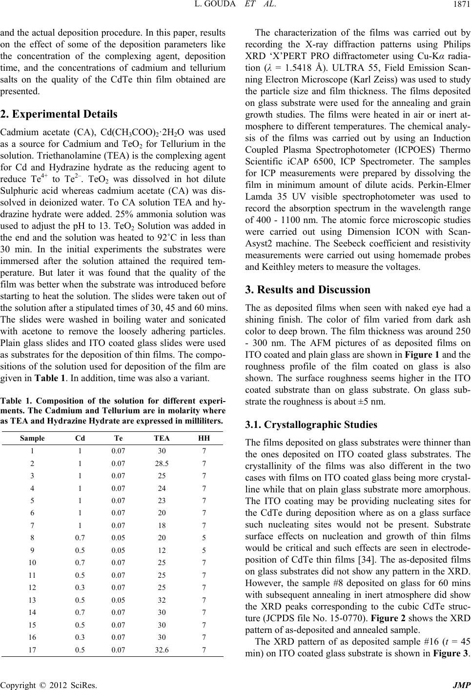 L. GOUDA ET AL. 1871 and the actual deposition procedure. In this paper, results on the effect of some of the deposition parameters like the concentration of the complexing agent, deposition time, and the concentrations of cadmium and tellurium salts on the quality of the CdTe thin film obtained are presented. 2. Experimental Details Cadmium acetate (CA), Cd(CH3COO)2·2H2O was used as a source for Cadmium and TeO2 for Tellurium in the solution. Triethanolamine (TEA) is the complexing agent for Cd and Hydrazine hydrate as the reducing agent to reduce Te4+ to Te2–. TeO2 was dissolved in hot dilute Sulphuric acid whereas cadmium acetate (CA) was dis- solved in deionized water. To CA solution TEA and hy- drazine hydrate were added. 25% ammonia solution was used to adjust the pH to 13. TeO2 Solution was added in the end and the solution was heated to 92˚C in less than 30 min. In the initial experiments the substrates were immersed after the solution attained the required tem- perature. But later it was found that the quality of the film was better when the substrate was introduced before starting to heat the solution. The slides were taken out of the solution after a stipulated times of 30, 45 and 60 mins. The slides were washed in boiling water and sonicated with acetone to remove the loosely adhering particles. Plain glass slides and ITO coated glass slides were used as substrates for the deposition of thin films. The compo- sitions of the solution used for deposition of the film are given in Table 1. In addition, time was also a variant. Table 1. Composition of the solution for different experi- ments. The Cadmium and Tellurium are in molarity where as TEA and Hydrazine Hydrate are express ed in milliliters. Sample Cd Te TEA HH 1 1 0.07 30 7 2 1 0.07 28.5 7 3 1 0.07 25 7 4 1 0.07 24 7 5 1 0.07 23 7 6 1 0.07 20 7 7 1 0.07 18 7 8 0.7 0.05 20 5 9 0.5 0.05 12 5 10 0.7 0.07 25 7 11 0.5 0.07 25 7 12 0.3 0.07 25 7 13 0.5 0.05 32 7 14 0.7 0.07 30 7 15 0.5 0.07 30 7 16 0.3 0.07 30 7 17 0.5 0.07 32.6 7 The characterization of the films was carried out by recording the X-ray diffraction patterns using Philips XRD ‘X’PERT PRO diffractometer using Cu-Kα radia- tion (λ = 1.5418 Å). ULTRA 55, Field Emission Scan- ning Electron Microscope (Karl Zeiss) was used to study the particle size and film thickness. The films deposited on glass substrate were used for the annealing and grain growth studies. The films were heated in air or inert at- mosphere to different temperatures. The chemical analy- sis of the films was carried out by using an Induction Coupled Plasma Spectrophotometer (ICPOES) Thermo Scientific iCAP 6500, ICP Spectrometer. The samples for ICP measurements were prepared by dissolving the film in minimum amount of dilute acids. Perkin-Elmer Lamda 35 UV visible spectrophotometer was used to record the absorption spectrum in the wavelength range of 400 - 1100 nm. The atomic force microscopic studies were carried out using Dimension ICON with Scan- Asyst2 machine. The Seebeck coefficient and resistivity measurements were carried out using homemade probes and Keithley meters to measure the voltages. 3. Results and Discussion The as deposited films when seen with naked eye had a shining finish. The color of film varied from dark ash color to deep brown. The film thickness was around 250 - 300 nm. The AFM pictures of as deposited films on ITO coated and plain glass are shown in Figure 1 and the roughness profile of the film coated on glass is also shown. The surface roughness seems higher in the ITO coated substrate than on glass substrate. On glass sub- strate the roughness is about ±5 nm. 3.1. Crystallographic Studies The films deposited on glass substrates were thinner than the ones deposited on ITO coated glass substrates. The crystallinity of the films was also different in the two cases with films on ITO coated glass being more crystal- line while that on plain glass substrate more amorphous. The ITO coating may be providing nucleating sites for the CdTe during deposition where as on a glass surface such nucleating sites would not be present. Substrate surface effects on nucleation and growth of thin films would be critical and such effects are seen in electrode- position of CdTe thin films [34]. The as-deposited films on glass substrates did not show any pattern in the XRD. However, the sample #8 deposited on glass for 60 mins with subsequent annealing in inert atmosphere did show the XRD peaks corresponding to the cubic CdTe struc- ture (JCPDS file No. 15-0770). Figure 2 shows the XRD pattern of as-deposited and annealed sample. The XRD pattern of as deposited sample #16 (t = 45 min) on ITO coated glass substrate is shown in Figure 3. Copyright © 2012 SciRes. JMP 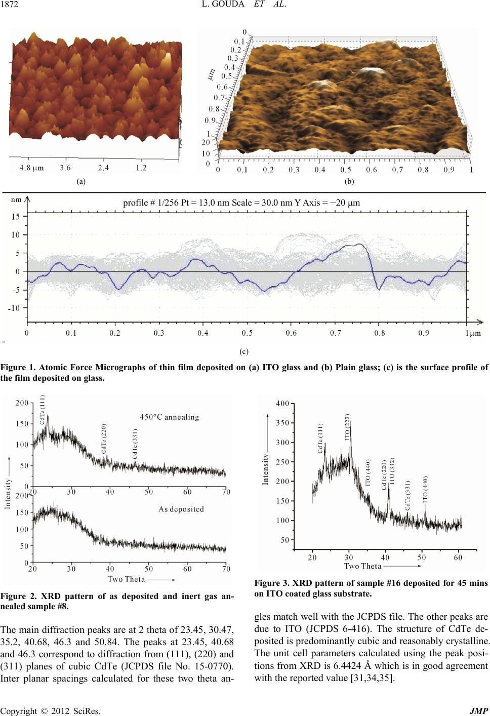 L. GOUDA ET AL. JMP 1872 (a) (b) profile # 1/256 Pt = 13.0 nm Scale = 30.0 nm Y Axis = – 20 μm (c) Figure 1. Atomic Force Micrographs of thin film deposited on (a) ITO glass and (b) Plain glass; (c) is the surface profile of the film deposited on glass. Figure 3. XRD pattern of sample #16 deposited for 45 mins on ITO coated glass substrate. Figure 2. XRD pattern of as deposited and inert gas an- nealed sample #8. gles match well with the JCPDS file. The other peaks are due to ITO (JCPDS 6-416). The structure of CdTe de- posited is predominantly cubic and reasonably crystalline. The unit cell parameters calculated using the peak posi- tions from XRD is 6.4424 Å which is in good agreement with the reported value [31,34,35]. The main diffraction peaks are at 2 theta of 23.45, 30.47, 35.2, 40.68, 46.3 and 50.84. The peaks at 23.45, 40.68 and 46.3 correspond to diffraction from (111), (220) and (311) planes of cubic CdTe (JCPDS file No. 15-0770). Inter planar spacings calculated for these two theta an- Copyright © 2012 SciRes. 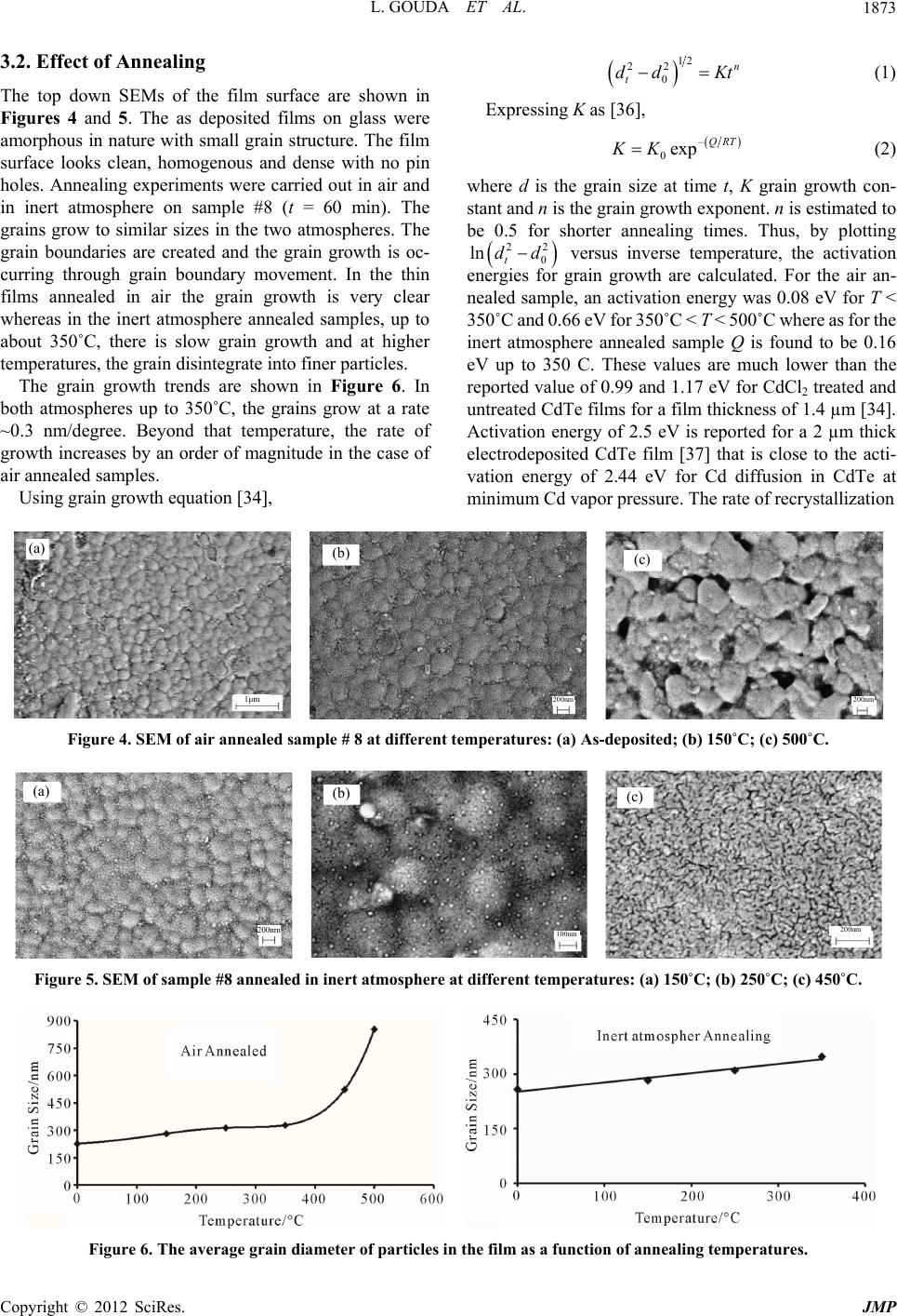 L. GOUDA ET AL. 1873 3.2. Effect of Annealing 12 22 0 n t dd Kt The top down SEMs of the film surface are shown in Figures 4 and 5. The as deposited films on glass were amorphous in nature with small grain structure. The film surface looks clean, homogenous and dense with no pin holes. Annealing experiments were carried out in air and in inert atmosphere on sample #8 (t = 60 min). The grains grow to similar sizes in the two atmospheres. The grain boundaries are created and the grain growth is oc- curring through grain boundary movement. In the thin films annealed in air the grain growth is very clear whereas in the inert atmosphere annealed samples, up to about 350˚C, there is slow grain growth and at higher temperatures, the grain disintegrate into finer particles. The grain growth trends are shown in Figure 6. In both atmospheres up to 350˚C, the grains grow at a rate ~0.3 nm/degree. Beyond that temperature, the rate of growth increases by an order of magnitude in the case of air annealed samples. Using grain growth equation [34], (1) Expressing K as [36], – 0exp QRT KK (2) where d is the grain size at time t, K grain growth con- stant and n is the grain growth exponent. n is estimated to be 0.5 for shorter annealing times. Thus, by plotting 22 ln dd 0t versus inverse temperature, the activation energies for grain growth are calculated. For the air an- nealed sample, an activation energy was 0.08 eV for T < 350˚C and 0.66 eV for 350˚C < T < 500˚C where as for the inert atmosphere annealed sample Q is found to be 0.16 eV up to 350 C. These values are much lower than the reported value of 0.99 and 1.17 eV for CdCl2 treated and untreated CdTe films for a film thickness of 1.4 µm [34]. Activation energy of 2.5 eV is reported for a 2 µm thick electrodeposited CdTe film [37] that is close to the acti- vation energy of 2.44 eV for Cd diffusion in CdTe at minimum Cd vapor pressure. The rate of recrystallization (a) 1 μ m (b) 200nm (c) 200nm Figure 4. SEM of air annealed sample # 8 at different temperatures: (a) As-deposited; (b) 150˚C; (c) 500˚C. (a) 200nm (b) 100nm (c) 200nm Figure 5. SEM of sample #8 annealed in inert atmosphere at different temperatures: (a) 150˚C; (b) 250˚C; (c) 450˚C. Figure 6. The average grain diameter of particles in the film as a function of annealing temperatures. Copyright © 2012 SciRes. JMP 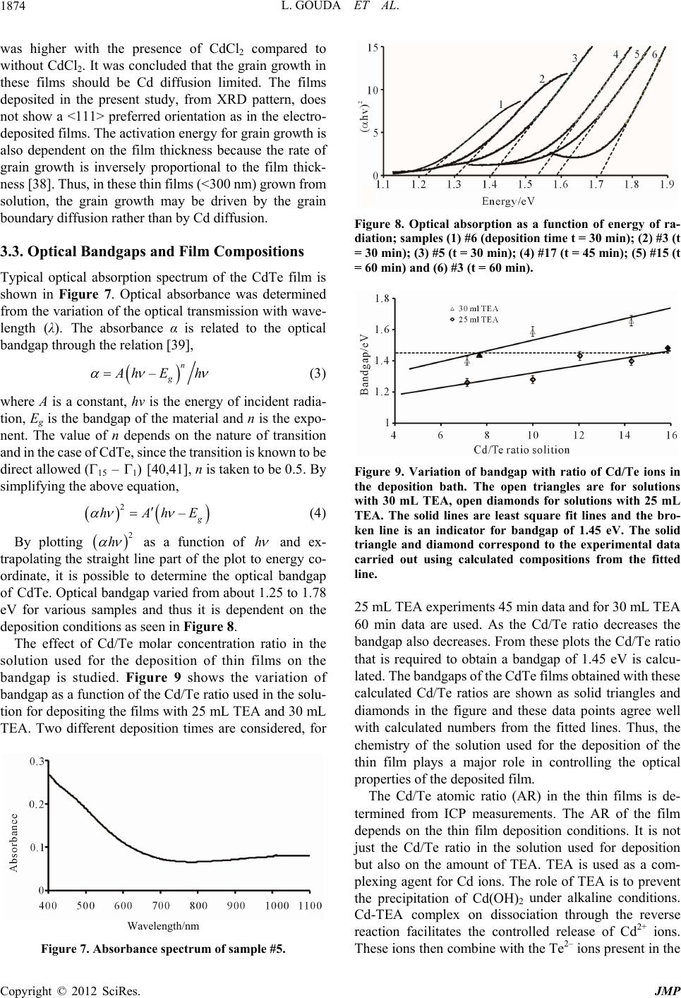 L. GOUDA ET AL. 1874 was higher with the presence of CdCl2 compared to without CdCl2. It was concluded that the grain growth in these films should be Cd diffusion limited. The films deposited in the present study, from XRD pattern, does not show a <111> preferred orientation as in the electro- deposited films. The activation energy for grain growth is also dependent on the film thickness because the rate of grain growth is inversely proportional to the film thick- ness [38]. Thus, in these thin films (<300 nm) grown from solution, the grain growth may be driven by the grain boundary diffusion rather than by Cd diffusion. 3.3. Optical Bandgaps and Film Compositions Typical optical absorption spectrum of the CdTe film is shown in Figure 7. Optical absorbance was determined from the variation of the optical transmission with wave- length (λ). The absorbance α is related to the optical bandgap through the relation [39], –n g A hE h – (3) where A is a constant, hν is the energy of incident radia- tion, Eg is the bandgap of the material and n is the expo- nent. The value of n depends on the nature of transition and in the case of CdTe, since the transition is known to be direct allowed (15 – 1) [40,41], n is taken to be 0.5. By simplifying the above equation, 2 g hAhE 2 h (4) By plotting h as a function of and ex- trapolating the straight line part of the plot to energy co- ordinate, it is possible to determine the optical bandgap of CdTe. Optical bandgap varied from about 1.25 to 1.78 eV for various samples and thus it is dependent on the deposition conditions as seen in Figure 8. The effect of Cd/Te molar concentration ratio in the solution used for the deposition of thin films on the bandgap is studied. Figure 9 shows the variation of bandgap as a function of the Cd/Te ratio used in the solu- tion for depositing the films with 25 mL TEA and 30 mL TEA. Two different deposition times are considered, for Wavelength/nm Figure 7. Absorbance spectrum of sample #5. Figure 8. Optical absorption as a function of energy of ra- diation; samples (1) #6 (deposition time t = 30 min); (2) #3 (t = 30 min); (3) #5 (t = 30 min); (4) #17 (t = 45 min); (5) #15 (t = 60 min) and (6) #3 (t = 60 min). Figure 9. Variation of bandgap with ratio of Cd/Te ions in the deposition bath. The open triangles are for solutions with 30 mL TEA, open diamonds for solutions with 25 mL TEA. The solid lines are least square fit lines and the bro- ken line is an indicator for bandgap of 1.45 eV. The solid triangle and diamond correspond to the experimental data carried out using calculated compositions from the fitted line. 25 mL TEA experiments 45 min data and for 30 mL TEA 60 min data are used. As the Cd/Te ratio decreases the bandgap also decreases. From these plots the Cd/Te ratio that is required to obtain a bandgap of 1.45 eV is calcu- lated. The bandgaps of the CdTe films obtained with these calculated Cd/Te ratios are shown as solid triangles and diamonds in the figure and these data points agree well with calculated numbers from the fitted lines. Thus, the chemistry of the solution used for the deposition of the thin film plays a major role in controlling the optical properties of the deposited film. The Cd/Te atomic ratio (AR) in the thin films is de- termined from ICP measurements. The AR of the film depends on the thin film deposition conditions. It is not just the Cd/Te ratio in the solution used for deposition but also on the amount of TEA. TEA is used as a com- plexing agent for Cd ions. The role of TEA is to prevent the precipitation of Cd(OH)2 under alkaline conditions. Cd-TEA complex on dissociation through the reverse reaction facilitates the controlled release of Cd2+ ions. These ions then combine with the Te2– ions present in the Copyright © 2012 SciRes. JMP 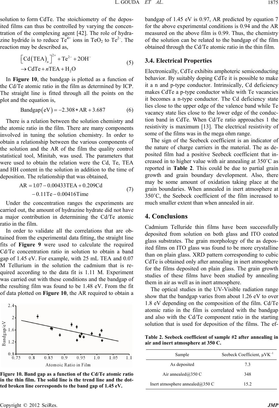 L. GOUDA ET AL. 1875 solution to form CdTe. The stoichiometry of the depos- ited films can thus be controlled by varying the concen- tration of the complexing agent [42]. The role of hydra- zine hydride is to reduce Te4+ ions in TeO2 to Te2–. The reaction may be described as, 2 Cd TEA CdTe TEA n n 2 2 Te 2OH H O AR 3.687 A 0.209Cd 16Time (5) In Figure 10, the bandgap is plotted as a function of the Cd/Te atomic ratio in the film as determined by ICP. The straight line is fitted through all the points on the plot and the equation is, BandgapeV2.308 (6) There is a relation between the solution chemistry and the atomic ratio in the film. There are many components involved in tuning the solution chemistry. In order to obtain a relationship between the various components of the solution and the AR of the film the quality control statistical tool, Minitab, was used. The parameters that were used to obtain the relation were the Cd, Te, TEA and HH content in the solution in addition to the time of deposition. The relationship that was obtained, AR1.07 0.00433TE 0.11Te0.004 (7) Under the concentration ranges the experiments are carried out, the amount of hydrazine hydrate did not have a major contribution in determining the Cd/Te atomic ratio in the film. In order to validate all the correlations that are ob- tained from the experimental data fitting, the straight line fits of Figure 9 were used to calculate the required Cd/Te concentration ratio in solution to obtain a band gap of 1.45 eV. For example, with 25 mL TEA and 0.07 M Tellurium in the solution the cadmium that is re- quired according to the data fit is 1.11 M. Experiment was carried out with these conditions and the bandgap of the resulting film was found to be 1.48 eV. From the fit of data plotted on Figure 10, the AR required to obtain a Figure 10. Band gap as a function of the Cd/Te atomic ratio in the thin film. The solid line is the trend line and the dot- ted broken line corresponds to the band gap of 1.45 eV. bandgap of 1.45 eV is 0.97, AR predicted by equation 7 for the above experimental conditions is 0.94 and the AR measured on the above film is 0.99. Thus, the chemistry of the solution can be related to the bandgap of the film obtained through the Cd/Te atomic ratio in the thin film. 3.4. Electrical Properties Electronically, CdTe exhibits amphoteric semiconducting behavior. By suitably doping CdTe it is possible to make it a n and p-type conductor. Intrinsically, Cd deficiency makes CdTe a p-type conductor while with Te vacancies it becomes a n-type conductor. The Cd deficiency state lies close to the upper edge of the valence band while Te vacancy state lies close to the lower edge of the conduc- tion band in CdTe. When Cd/Te ratio approaches 1 the resistivity is maximum [13]. The electrical resistivity of some of the films was in the mega ohm range. The sign of the Seebeck coefficient is an indicator of the nature of charge carriers in the material. The as de- posited film had a positive Seebeck coefficient that in- creased in to higher value with air annealing at 350˚C as reported in Table 2. This could be due to partial grain growth and grain boundary development. Also, there may be some amount of oxidation taking place at the grain boundaries. When annealed in inert atmosphere at 350˚C, the Seebeck coefficient of the film increased to much smaller extent than when annealed in air. 4. Conclusions Cadmium Telluride thin films have been successfully deposited from solution on both glass and ITO coated glass substrates. The grain morphology of the as depos- ited films on ITO glass was found to be more crystalline than on plain glass. XRD pattern corresponding to cubic CdTe is obtained only after annealing in inert atmosphere for the films deposited on plain glass. The grain growth studies of these films have been studied by annealing them in air as well as in inert atmosphere. The optical studies in the UV-Visible radiation range show that the bandgap varies from about 1.26 eV to over 1.8 eV depending on the composition of the film. Cd/Te atomic ratio in the film is correlated with the bandgap and also with the Cd/Te component ratio in the starting solution that is used for deposition of the films. The ef- Table 2. Seebeck coefficient of sample #2 after annealing in air and inert atmosphere at 350 C. Sample Seebeck Coefficient, μVK–1 As deposited 7.3 Air annealed@350 C 348 Inert atmosphere annealed@350 C 15.2 Copyright © 2012 SciRes. JMP 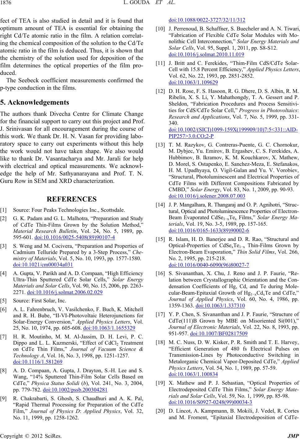 L. GOUDA ET AL. 1876 fect of TEA is also studied in detail and it is found that optimum amount of TEA is essential for obtaining the right Cd/Te atomic ratio in the film. A relation correlat- ing the chemical composition of the solution to the Cd/Te atomic ratio in the film is deduced. Thus, it is shown that the chemistry of the solution used for deposition of the film determines the optical properties of the film pro- duced. The Seebeck coefficient measurements confirmed the p-type conduction in the films. 5. Acknowledgements The authors thank Divecha Centre for Climate Change for the financial support to carry out this project and Prof. J. Srinivasan for all encouragement during the course of this work. We thank Dr. H. N. Vasan for providing labo- ratory space to carry out experiments without this help the work would not have taken shape. We also would like to thank Dr. Vasantacharya and Mr. Jarali for help with electrical and optical measurements. We acknowl- edge the help of Mr. Sathyanarayana and Prof. T. N. Guru Row in SEM and XRD characterization. REFERENCES [1] Source: Four Peaks Technologies Inc., Scottsdale. [2] G. K. Padam and G. L. Malhotra, “Preparation and Study of CdTe Thin-Films Grown by the Solution Method,” Material Research Bulletin, Vol. 24, No. 5, 1989, pp. 595-601. doi:10.1016/0025-5408(89)90107-4 [3] S. Weng and M. Cocivera, “Preparation and Properties of Cadmium Telluride Prepared by a 3-Step Process,” Che- mistry of Materials, Vol. 5, No. 10, 1993, pp. 1577-1580. doi:10.1021/cm00034a031 [4] A. Gupta, V. Parikh and A. D. Compaan, “High Efficiency Ultra-Thin Sputtered CdTe Solar Cells,” Solar Energy Materials and Solar Cells, Vol. 90, No. 15, 2006, pp. 2263- 2271. doi:10.1016/j.solmat.2006.02.029 [5] Source: First Solar, Inc. [6] A. L. Fahrenbruch, V. Vasilchenko, F. Buch, K. Mitchell and R. H. Bube, “II-VI-Photovoltaic Heterojunctions for Solar-Energy Conversion,” Applied Physics Letters, Vol. 25, No. 10, 1974, pp. 605-608. doi:10.1063/1.1655329 [7] H. R. Moutinho, M. M. Al-Jassim, D. H. Levi, P. C. Dippo and L. L. Kazmerski, “Effect of CdCl2 Treatment on CdTe Thin Films,” Journal of Vacuum Science & Technology A, Vol. 16, No. 3, 1998, pp. 1251-1257. doi:10.1116/1.581269 [8] A. D. Compaan, A. Gupta, J. Drayton, S.-H. Lee and S. Wang, “14% Sputtered Thin-Film Solar Cells Based on CdTe,” Physica Status Solidi (b), Vol. 241, No. 3, 2004, pp. 779-782. doi:10.1002/pssb.200304281 [9] R. Chakrabarti, S. Ghosh, S. Chaudhuri and A. K. Pal, “Rapid Thermal Processing for Preparation of the CdTe Film,” Journal of Physics D: Applied Physics, Vol. 32, No. 11, 1999, pp. 1258-1262. doi:10.1088/0022-3727/32/11/312 [10] J. Perrenoud, B. Schaffner, S. Buecheler and A. N. Tiwari, “Fabrication of Flexible CdTe Solar Modules with Mo- nolithic Cell Interconnection,” Solar Energy Materials and Solar Cells, Vol. 95, Suppl. 1, 2011, pp. S8-S12. doi:10.1016/j.solmat.2010.11.019 [11] J. Britt and C. Ferekides, “Thim-Film CdS/CdTe Solar- Cell with 15.8 Percent Efficiency,” Applied Physics Letters, Vol. 62, No. 22, 1993, pp. 2851-2852. doi:10.1063/1.109629 [12] D. H. Rose, F. S. Hasoon, R. G. Dhere, D. S. Albin, R. M. Ribelin, X. S. Li, Y. Mahathongdy, T. A. Gessert and P. Sheldon, “Fabrication Procedures and Process Sensitivi- ties for CdS/CdTe Solar Cell,” Progress in Photovoltaics: Research and Applications, Vol. 7, No. 5, 1999, pp. 331- 340. doi:10.1002/(SICI)1099-159X(199909/10)7:5<331::AID- PIP257>3.0.CO;2-P [13] T. M. Razykov, G. Contreras-Puente, G. C. Chornokur, M. Dybjec, Yu. Emirov, B. Ergashev, C. S. Ferekides, A. Hubbimov, B. Ikramov, K. M. Kouchkarov, X. Mathew, D. Morel, S. Ostapenko, E. Sanchez-Meza, E. Stefanakos, H. M. Upadhyaya, O. Vigil-Galan and Yu. V. Vorobiev, “Structural, Photoluminescent and Electrical Properties of CdTe Films with Different Compositions Fabricated by CMBD,” Solar Energy, Vol. 83, No. 1, 2009, pp. 90-93. doi:10.1016/j.solener.2008.07.003 [14] J. P. Mangalhara, R. Thangaraj and O. P. Agnihotri, “Struc- tural, Optical and Photoluminescence Properties of Electron- Beam Evaporated CdSe1−xTex Films,” Solar Energy Ma- terials, Vol. 19, No. 3-5, 1989, pp. 157-165. doi:10.1016/0165-1633(89)90002-6 [15] R. Islam, H. D. Banerjee and D. R. Rao, “Structural and Optical-Properties of CdSexTe1−x Thin-Films Grown by Electron-Beam Evaporation,” Thin Solid Films, Vol. 266, No. 2, 1995, pp. 215-218. doi:10.1016/0040-6090(96)80027-7 [16] S. Sivananthan, X. Chu, J. Reno and J. P. Faurie, “Re- lation between Crystallographic Orientation and the Con- densation Coefficients of Hg, Cd, and Te during Mole- cular-Beam-Epitaxial Growth of Hg1−xCdxTe and CdTe,” Journal of Applied Physics, Vol. 60, No. 4, 1986, pp. 1359-1363. doi:10.1063/1.337310 [17] Y. P. Chen, S. Sivananthan and J. P. Faurie, “Structure of CdTe(111)B Grown by MBE on Misoriented Si(001),” Journal of Electronic Materials, Vol. 22, No. 8, 1993, pp. 951-957. doi:10.1007/BF02817509 [18] M. C. Nuss, D. W. Kisker, P. R. Smith and T. E. Harvey, “Efficient Generation of 480 fs Electrical Pulses on Transmission-Lines by Photoconductive Switching in Metalorganic Chemical Vapor-Deposited CdTe,” Applied Physics Letters, Vol. 54, No. 1, 1989, pp. 57-59. doi:10.1063/1.100834 [19] X. Mathew and P. J. Sebastian, “Optical Properties of Electrodeposited CdTe Thin Films,” Solar Energy Mate- rials and Solar Cells, Vol. 59, No. 1, 1999, pp. 85-98. doi:10.1016/S0927-0248(99)00034-3 [20] D. Lincot, A. Kampmann, B. Mokili, J. Vedel, R. Cortes and M. Froment, “Epitaxial Electrodeposition of CdTe- Copyright © 2012 SciRes. JMP  L. GOUDA ET AL. Copyright © 2012 SciRes. JMP 1877 Films on INP from Aqueous-Solutions—Role of a Che- mically Deposited CdS Intermediate Layer,” Applied Phy- sics Letters, Vol. 67, No. 2358, 1995, pp. 2355-2357. doi:10.1063/1.114343 [21] S.-Y. Yang, J.-C. Chou and H.-Y. Ueng, “Influence of Electrodeposition Potential and Heat Treatment on Struc- tural Properties of CdTe Films,” Thin Solid Films, Vol. 518, No. 15, 2010, pp. 4197-4202. doi:10.1016/j.tsf.2009.12.077 [22] K. Murase, M. Matsui, M. Miyake, T. Hirato and Y. Awakura, “Photoassisted Electrodeposition of CdTe Layer from Ammoniacal Basic Aqueous Solutions,” Journal of the Electrochemical Society, Vol. 150, No. 1, 2003, pp. C44-C51. doi:10.1149/1.1526110 [23] G. Hodes, “Chemical Solution Deposition of Semicon- ductor Films,” Marcel Dekker Inc., New York, 2002. doi:10.1201/9780203909096 [24] T. P. Niesen and M. R. De Guire, “Review: Deposition of Ceramic Thin Films at Low Temperatures from Aqueous Solutions,” Journal of Electroceramics, Vol. 6, No. 3, 2001, pp. 169-207. doi:10.1023/A:1011496429540 [25] J. Han, C. Spanheimer, G. Haindl, G. Fu, V. Krishnaku- mar, J. Schaffner, C. Fan, K. Zhao, A. Klein and W. Jae- germann, “Optimized Chemical Bath Deposited CdS Layers for the Improvement of CdTe Solar Cells,” Solar Energy Materials and Solar Cells, Vol. 95, No. 3, 2011, pp. 816-820. doi:10.1016/j.solmat.2010.10.027 [26] N. G. Dhere, D. L. Waterhouse, K. B. Sundaram, O. Melendez, N. R. Parikh and B. Patnaik, “Studies on Chemical Bath Deposited Cadmium-Sulfide Films by Buffer Solution Technique,” Journal of Materials Science: Materials in Electronics, Vol. 6, No. 1, 1995, pp. 52-59. doi:10.1007/BF00208134 [27] J. Y. Choi, K.-J. Kim, J.-B. Yoo and D. Kim, “Properties of Cadmium Sulfide Thin Films Deposited by Chemical Bath Deposition with Ultrasonication,” Solar Energy, Vol. 64, No. 1-3, 1998, pp. 41-47. doi:10.1016/S0038-092X(98)00047-4 [28] F. Ouachtari, A. Rmili, S. E. Elidrissi, A. Bouaoud, H. Erguig and P. Elies, “Influence of Bath Temperature, Deposition Time and [S]/[Cd] Ratio on the Structure, Surface Morphology, Chemical Composition and Optical Properties of CdS Thin Films Elaborated by Chemical Bath Deposition,” Journal of Modern Physics, Vol. 2, No. 9, 2011, pp. 1073-1082. doi:10.4236/jmp.2011.29131 [29] G. K. Padam and G. L. Malhotra, “Preparation and Study of CdTe Thin-Films Grown by the Solution Method,” Materials and Research Bulletin, Vol. 24, 1989, pp. 595- 601. doi:10.1016/0025-5408(89)90107-4 [30] N. P. Klochko, N. D. Volkova, M. M. Kharchenko and V. R. Kopach, “Contact Electro Deposition of CdTe Thin- Films,” Functional Materials, Vol. 16, 2009, pp. 190- 191. [31] G. Khrypunov, N. Klochko, N. Volkova, V. Lyubov and T. Li, “Effect of CdCl2 Treatment on Properties of CdTe- Based Solar Cells Prepared by Physical Vapor Deposition and Close-Spaced Sublimation Methods,” Japanese Jour- nal of Applied Physics, Vol. 50, No. 5, 2011, pp. 05FH01- 05FH02. [32] S. Deivanayaki, P. Jayamurugan, R. Mariappan and V. Ponnuswamy, “Optical and Structural Characterization of CdTe Thin Films by Chemical Bath Deposition Tech- nique,” Chalcogenide Letters, Vol. 7, No. 3, 2010, pp. 159-163. [33] K. M. Garadkar, S. J. Pawar, P. P. Hankare and A. A. Patil, “Effect of Annealing on Chemically Deposited Polycrystalline CdTe Thin Films,” Journal of Alloys and Compounds, Vol. 491, No. 1-2, 2010, pp. 77-80. doi:10.1016/j.jallcom.2009.10.146 [34] J. P. Enriquez and X. Mathew, “Anneal Induced Recry- stallization of CdTe Films Electrodeposited on Stainless Steel Foil: The Effect of CdCl2,” Journal of Materials Science: Materials in Electronics, Vol. 16, No. 9, 2005, pp. 617-621. doi:10.1007/s10854-005-3237-9 [35] I. Spinulescu-Carnaru, “Growth of Hexagonal Crystallites in CdTe Thin Films,” Physica Status Solidi, Vol. 15, No. 2, 1966, pp. 761-765. doi:10.1002/pssb.19660150237 [36] R. Chaim, “Activation Energy and Y-Grain Growth in Nanocrystalline TZP Ceramics,” Materials Science and Engineering A, Vol. 486, 2008, pp. 439-446. doi:10.1016/j.msea.2007.09.022 [37] B. Qi, D. Kim, D. L. Williamson and J. U. Trefny, “Effects of Postdeposition Heat-Treatment on Morpho- logy and Microstructure of CdTe Grown by Electro- deposition,” Journal of Electrochemical Society, Vol. 143, No. 2, 1996, pp. 517-523. doi:10.1149/1.1836474 [38] C. V. Thompson, “Secondary Grain-Growth in Thin- Films of Semiconductors—Theoretical Aspects,” Journal of Applied Physics, Vol. 58, No. 2, 1985, pp. 763-772. doi:10.1063/1.336194 [39] J. Tauc and A. Menth, “States in the Gap,” Journal of Non-Crystalline Solids, Vol. 8-10, 1972, pp. 569-585. doi:10.1016/0022-3093(72)90194-9 [40] M. Cardona and D. L. Greenaway, “Fundamental Reflec- tivity and Band Structure of ZnTe, CdTe, and HgTe,” Physical Review Letters, Vol. 131, No. 1, 1963, pp. 98- 103. [41] N. A. Noor, W. Tahir, F. Aslam and A. Shaukat, “Ab Initio Study of Structural, Electronic and Optical Properties of Be-doped CdS, CdSe and CdTe Compounds,” Physica B, Vol. 407, No. 6, 2012, pp. 943-952. doi:10.1016/j.physb.2011.12.107 [42] K. V. Krishna and V. Dutta, “Spray Deposition of CdTe-Te Thin Films using Ethylene-Diamine-Tetra-Acetic Acid as a Complexing Agent in the Precursor Solution,” Solar Energy Materials and Solar Cells, Vol. 80, No. 2, 2003, pp. 247-256. doi:10.1016/j.solmat.2003.05.001 |