

Paper Menu >>
Journal Menu >>
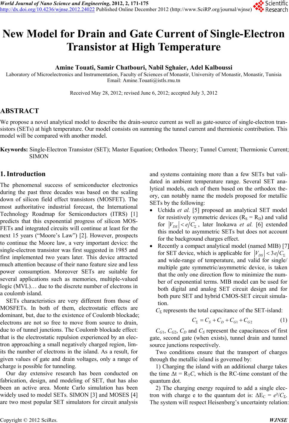 World Journal of Nano Science and Engineering, 2012, 2, 171-175 http://dx.doi.org/10.4236/wjnse.2012.24022 Published Online December 2012 (http://www.SciRP.org/journal/wjnse) New Model for Drain and Gate Current of Single-Electron Transistor at High Temperature Amine Touati, Samir Chatbouri, Nabil Sghaier, Adel Kalboussi Laboratory of Microelectronics and Instrumentation, Faculty of Sciences of Monastir, University of Monastir, Monastir, Tunisia Email: [email protected] Received May 28, 2012; revised June 6, 2012; accepted July 3, 2012 ABSTRACT We propose a novel analytical model to describe the drain-source current as well as gate-source of single-electron tran- sistors (SETs) at high temperature. Our model consists on summing the tunnel current and thermionic contribution. This model will be compared with another model. Keywords: Single-Electron Transistor (SET); Master Equation; Orthodox Theory; Tunnel Current; Thermionic Current; SIMON 1. Introduction The phenomenal success of semiconductor electronics during the past three decades was based on the scaling down of silicon field effect transistors (MOSFET). The most authoritative industrial forecast, the International Technology Roadmap for Semiconductors (ITRS) [1] predicts that this exponential progress of silicon MOS- FETs and integrated circuits will continue at least for the next 15 years (“Moore’s Law”) [2]. However, prospects to continue the Moore law, a very important device: the single-electron transistor was first suggested in 1985 and first implemented two years later. This device attracted much attention because of their nano feature size and less power consumption. Moreover SETs are suitable for several applications such as memories, multiple-valued logic (MVL)… due to the discrete number of electrons in a coulomb island. SETs characteristics are very different from those of MOSFETs. In both of them, electrostatic effects are dominant, but, due to the existence of Coulomb blockade; electrons are not so free to move from source to drain, due to of tunnel junctions. The Coulomb blockade effect: that is the electrostatic repulsion experienced by an elec- tron approaching a small negatively charged region, lim- its the number of electrons in the island. As a result, for given values of gate and drain voltages, only a range of charge is possible for tunneling. Our day extensive research has been conducted on fabrication, design, and modeling of SET, that has also been an active area. Monte Carlo simulation has been widely used to model SETs. SIMON [3] and MOSES [4] are two most popular SET simulators for circuit analysis and systems containing more than a few SETs but vali- dated in ambient temperature range. Several SET ana- lytical models, each of them based on the orthodox the- ory, can notably name the models proposed for metallic SETs by the following: Uchida et al. [5] proposed an analytical SET model for resistively symmetric devices (RS = RD) and valid for DS VeC , later Inokawa et al. [6] extended this model to asymmetric SETs but does not account for the background charges effect. Recently a compact analytical model (named MIB) [7] for SET device, which is applicable for 3 DS VeC and wide-range of temperature, and valid for single/ multiple gate symmetric/asymmetric device, is taken that the only one direction flow to minimize the num- ber of exponential terms. MIB model can be used for both digital and analog SET circuit design and for both pure SET and hybrid CMOS-SET circuit simula- tion. CΣ represents the total capacitance of the SET-island: 1SDGG CCCC C 2 (1) CG1, CG2, CD and CS represent the capacitances of first gate, second gate (when exists), tunnel drain and tunnel source junctions respectively. Two conditions ensure that the transport of charges through the metallic island is governed by: 1) Charging the island with an additional charge takes the time Δt = RTC, which is the RC-time constant of the quantum dot. 2) The charging energy required to add a single elec- tron with charge e to the quantum dot is: ΔEC = e²/CΣ. The system will respect Heisenberg’s uncertainty relation: C opyright © 2012 SciRes. WJNSE 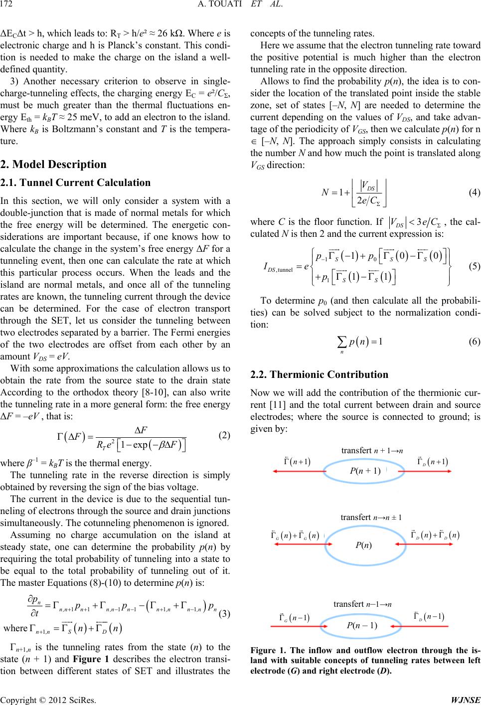 A. TOUATI ET AL. 172 ΔECΔt > h, which leads to: RT > h/e² ≈ 26 kΩ. Where e is electronic charge and h is Planck’s constant. This condi- tion is needed to make the charge on the island a well- defined quantity. 3) Another necessary criterion to observe in single- charge-tunneling effects, the charging energy EC = e²/CΣ, must be much greater than the thermal fluctuations en- ergy Eth = kBT ≈ 25 meV, to add an electron to the island. Where kB is Boltzmann’s constant and T is the tempera- ture. 2. Model Description 2.1. Tunnel Current Calculation In this section, we will only consider a system with a double-junction that is made of normal metals for which the free energy will be determined. The energetic con- siderations are important because, if one knows how to calculate the change in the system’s free energy ΔF for a tunneling event, then one can calculate the rate at which this particular process occurs. When the leads and the island are normal metals, and once all of the tunneling rates are known, the tunneling current through the device can be determined. For the case of electron transport through the SET, let us consider the tunneling between two electrodes separated by a barrier. The Fermi energies of the two electrodes are offset from each other by an amount VDS = eV. With some approximations the calculation allows us to obtain the rate from the source state to the drain state According to the orthodox theory [8-10], can also write the tunneling rate in a more general form: the free energy ΔF = –eV , that is: 21exp T F FRe F (2) where β–1 = kBT is the thermal energy. The tunneling rate in the reverse direction is simply obtained by reversing the sign of the bias voltage. The current in the device is due to the sequential tun- neling of electrons through the source and drain junctions simultaneously. The cotunneling phenomenon is ignored. Assuming no charge accumulation on the island at steady state, one can determine the probability p(n) by requiring the total probability of tunneling into a state to be equal to the total probability of tunneling out of it. The master Equations (8)-(10) to determine p(n) is: 1111 11 1 where n n,nnn,nnn ,nn ,nn n,n SD ppp t nn p (3) Γn+1,n is the tunneling rates from the state (n) to the state (n + 1) and Figure 1 describes the electron transi- tion between different states of SET and illustrates the concepts of the tunneling rates. Here we assume that the electron tunneling rate toward the positive potential is much higher than the electron tunneling rate in the opposite direction. Allows to find the probability p(n), the idea is to con- sider the location of the translated point inside the stable zone, set of states [–N, N] are needed to determine the current depending on the values of VDS, and take advan- tage of the periodicity of VGS, then we calculate p(n) for n [–N, N]. The approach simply consists in calculating the number N and how much the point is translated along VGS direction: 12 DS V NeC (4) where C is the floor function. If 3 DS VeC , the cal- culated N is then 2 and the current expression is: 10 ,tunnel 1 10 11 SSS DS SS pp Ie p 0 (5) To determine p0 (and then calculate all the probabili- ties) can be solved subject to the normalization condi- tion: 1 n pn (6) 2.2. Thermionic Contribution Now we will add the contribution of the thermionic cur- rent [11] and the total current between drain and source electrodes; where the source is connected to ground; is given by: 1n 1 Dn GG nn DD nn 1 Dn 1 Gn transfert n + 1→n transfert n→n ± 1 transfert n – 1→n P(n + 1) P(n) P(n – 1) Figure 1. The inflow and outflow electron through the is- land with suitable concepts of tunneling rates between left electrode (G) and right electrode (D). Copyright © 2012 SciRes. WJNSE 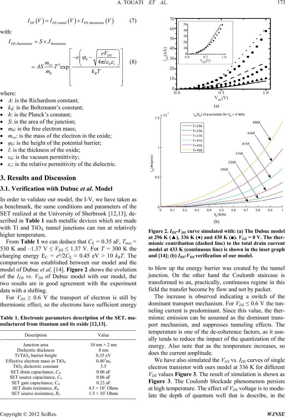 A. TOUATI ET AL. 173 ,tunnel ,thermionicDS DSDS I VI VIV (7) with: ,thermionic thermionic 0 0 2 0 4π exp DS DS r ox B ISJ eV el m AS T mkT (8) where: A: is the Richardson constant; kB: is the Boltzmann’s constant; h: is the Planck’s constant; S: is the area of the junction; m0: is the free electron mass; mox: is the mass of the electron in the oxide; φ0: is the height of the potential barrier; l: is the thickness of the oxide; ε0: is the vacuum permittivity; εr: is the relative permittivity of the dielectric. 3. Results and Discussion 3.1. Verification with Dubuc et al. Model In order to validate our model, the I-V, we have taken as a benchmark, the same conditions and parameters of the SET realized at the University of Sherbrook [12,13], de- scribed in Table 1 such metallic devices which are made with Ti and TiOX tunnel junctions can run at relatively higher temperature. From Table 1 we can deduce that CΣ = 0.35 aF, Tmax = 530 K and –1.37 V ≤ VDS ≤ 1.37 V. For T = 300 K the charging energy EC = e²/2CΣ ≈ 0.45 eV > 10 kBT. The comparison was established between our model and the model of Dubuc et al. [14]. Figure 2 shows the evolution of the IDS vs. VDS of Dubuc model with our model, the two results are in good agreement with the experiment data with a shifting. For VDS ≥ 0.6 V the transport of electron is still by thermionic effect, so the electrons have sufficient energy Table 1. Electronic parameters description of the SET, ma- nufactured from titanium and its oxide [12,13]. Description Value Junction area Dielectric thickness Ti/TiOX barrier height Effective electron mass in TiOX TiOX dielectric constant SET drain capacitance, CD SET source capacitance, CS SET gate capacitance, CG SET drain resistance, RD SET source resistance, RS 10 nm × 2 nm 8 nm 0.35 eV 0.40*m0 3.5 0.06 aF 0.06 aF 0.23 aF 4.5 × 10⁷ Ohms 1.5 × 10⁷ Ohms (a) (b) Figure 2. IDS-VDS curve simulated with: (a) The Dubuc model at 296 K (▲), 336 K (●) and 430 K (■). VGS = 0 V. The ther- mionic contribution (dashed line) to the total drain current model at 433 K (continuous line) is shown in the inset graph and [14]; (b) IDS-VDS verification of our model. to blow up the energy barrier was created by the tunnel junction. On the other hand the Coulomb staircase is transformed to an, practically, continuous regime in this field the transfer become by flow and not by packet. The increase is observed indicating a switch of the dominant transport mechanism. For VDS ≤ 0.6 V the tun- neling current is predominant. Since this value, the ther- mionic emission can be assumed as the dominant trans- port mechanism, and suppresses tunneling effects. The temperature is one of the de-coherence factors, as it usu- ally tends to reduce the impact of the quantization of the energy. Also note that as the temperature increases, so does the current amplitude. We have also simulated the VGS vs. IDS curves of single electron transistor with ours model at 336 K for different VDS values Figure 3. The result of simulation is shown as Figure 3. The Coulomb blockade phenomenon persists at high temperature. The effect of VDS voltage is to modu- late the depth of quantum well that is describe, in the Copyright © 2012 SciRes. WJNSE 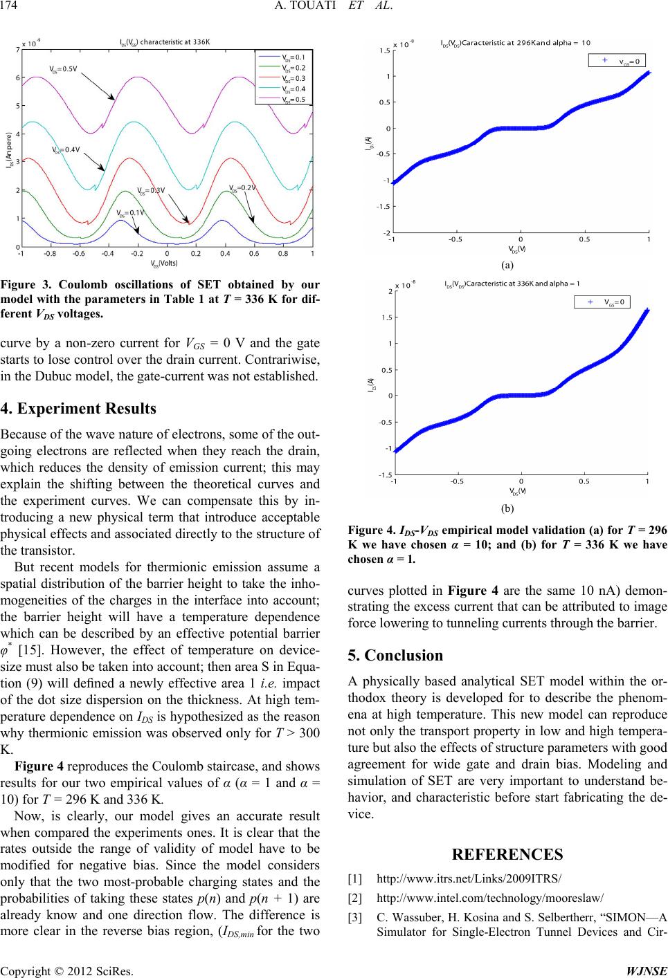 A. TOUATI ET AL. 174 Figure 3. Coulomb oscillations of SET obtained by our model with the parameters in Table 1 at T = 336 K for dif- ferent VDS voltages. curve by a non-zero current for VGS = 0 V and the gate starts to lose control over the drain current. Contrariwise, in the Dubuc model, the gate-current was not established. 4. Experiment Results Because of the wave nature of electrons, some of the out- going electrons are reflected when they reach the drain, which reduces the density of emission current; this may explain the shifting between the theoretical curves and the experiment curves. We can compensate this by in- troducing a new physical term that introduce acceptable physical effects and associated directly to the structure of the transistor. But recent models for thermionic emission assume a spatial distribution of the barrier height to take the inho- mogeneities of the charges in the interface into account; the barrier height will have a temperature dependence which can be described by an effective potential barrier φ* [15]. However, the effect of temperature on device- size must also be taken into account; then area S in Equa- tion (9) will defined a newly effective area 1 i.e. impact of the dot size dispersion on the thickness. At high tem- perature dependence on IDS is hypothesized as the reason why thermionic emission was observed only for T > 300 K. Figure 4 reproduces the Coulomb staircase, and shows results for our two empirical values of α (α = 1 and α = 10) for T = 296 K and 336 K. Now, is clearly, our model gives an accurate result when compared the experiments ones. It is clear that the rates outside the range of validity of model have to be modified for negative bias. Since the model considers only that the two most-probable charging states and the probabilities of taking these states p(n) and p(n + 1) are already know and one direction flow. The difference is more clear in the reverse bias region, (IDS,min for the two (a) (b) Figure 4. IDS-VDS empirical model validation (a) for T = 296 K we have chosen α = 10; and (b) for T = 336 K we have chosen α = 1. curves plotted in Figure 4 are the same 10 nA) demon- strating the excess current that can be attributed to image force lowering to tunneling currents through the barrier. 5. Conclusion A physically based analytical SET model within the or- thodox theory is developed for to describe the phenom- ena at high temperature. This new model can reproduce not only the transport property in low and high tempera- ture but also the effects of structure parameters with good agreement for wide gate and drain bias. Modeling and simulation of SET are very important to understand be- havior, and characteristic before start fabricating the de- vice. REFERENCES [1] http://www.itrs.net/Links/2009ITRS/ [2] http://www.intel.com/technology/mooreslaw/ [3] C. Wassuber, H. Kosina and S. Selbertherr, “SIMON—A Simulator for Single-Electron Tunnel Devices and Cir- Copyright © 2012 SciRes. WJNSE  A. TOUATI ET AL. Copyright © 2012 SciRes. WJNSE 175 cuits,” IEEE Transactions on Computer-Aided Design of Integrated Circuits and Systems, Vol. 16, No. 9, 1997, pp. 937-944. doi:10.1109/43.658562 [4] R. H. Chen, “MOSES: A General Monte Carlo Simulator for Single-Electronic Circuits,” The Electrochemical So- ciety, Vol. 96, 1996, p. 576. [5] K. Uchida, K. Matsuzawa, J. Koga, R. Ohba, S. Takagi and A. Toriumi, “Analytical Single-Electron Transistor (SET) Model for Design and Analysis of Realistic SET Circuits,” Japanese Journal of Applied Physics, Vol. 39, No. 4B, 2000, pp. 2321-2324. doi:10.1143/JJAP.39.2321 [6] H. Inokawa and Y. Takahashi, “A Compact Analytical Model for Asymmetric Single-Electron Tunneling Tran- sistors,” IEEE Transactions on Electron Devices, Vol. 50, No. 2, 2003, pp. 455-461. doi:10.1109/TED.2002.808554 [7] S. Mahapatra, V. Vaish, C. Wasshuber, K. Banerjee and A. M. Ionescu, “Analytical Modeling of Single Electron Transistor for Hybrid CMOS-SET Analog IC Design,” IEEE Transactions on Electron Devices, Vol. 51, No. 11, 2004, pp. 1772-1782. doi:10.1109/TED.2004.837369 [8] T. Dittrich, P. Hänggie, G. L. Ingold, B. Kramer, G. Schön and W. Zwerger, “Quantum Transport and Dissipation,” Wiley-VCH, Berlin, 1998. [9] C. Delerue and M. Lanno, “Nanostructures: Theory and Modelling,” Springer, Berlin, 2004. [10] D. V. Averin and K. K. Likharev, “Mesoscopic Phenom- ena in Solids,” Elsevier, Amsterdam, 1991. [11] S. M. Sze and K. K. Ng, “Physics of Semiconductor De- vices,” 3rd Edition, John Wiley & Sons, New Jersey, 2007. [12] C. Dubuc, J. Beauvais and D. Drouin, “A Nanodamas- cene Process for Advanced Single-Electron Transistor Fabrication,” IEEE Transactions on Nanotechnology, Vol. 7, No. 1, 2008, pp. 68-73. [13] A. Beaumont, C. Dubuc, J. Beauvais and D. Drouin, “A Nanodamascene Process for Advanced Single-Electron Transistor Fabrication,” IEEE Transactions on Nanotech- nologyon, Vol. 7, No. 1, 2009, pp. 68-73. doi:10.1109/TNANO.2007.91343010 [14] C. Dubuc, A. Beaumont, J. Beauvais and D. Drouin, “Current Conduction Models in the High Temperature Single-Electron Transistor,” Solid-State Electronics, Vol. 53, No. 5, 2009, pp. 478-482. doi:10.1016/j.sse.2009.03.003 [15] J. H. Werner and H. H. Guttler, “Barrier Inhomogeneities at Schottky Contacts,” Journal of Applied Physics, Vol. 69, No. 3, 1991, pp. 1522-1533. doi:10.1063/1.347243 |