

Paper Menu >>
Journal Menu >>
 Journal of Electromagnetic Analysis and Applications, 2012, 4, 423-425 http://dx.doi.org/10.4236/jemaa.2012.410058 Published Online October 2012 (http://www.SciRP.org/journal/jemaa) 423 Effect of the Width of the NRD Waveguide on the S Parameter of a Pass Band Filter Harizi Hanen1, Lattrach Lassaad1, Gharssallah Ali1, Garbi Abdelhafedh2 1Unit of Research Circuits and Electronics Systems High Frequency, Faculty of Science, University El Manar, Tunis, Tunisia; 2Laboratory of Research Circuits and Electronics Systems High Frequency, Faculty of Science, University El Manar, Tunis, Tunisia. Email: [email protected] Received July 9th, 2012; revised August 18th, 2012; accepted September 3rd, 2012 ABSTRACT In this paper, we present a design of a non-radiative dielectric waveguide band pass filter based on hybrid architecture of micro-strip line and non-radiative dielectric waveguide. The simulation with high frequency structure simulator (HFSS) three dimensional analyses are presented, also the influence of the feeding transitions for circuit design is studied . The aim of this work was to study the influence of the width of the NRD waveguide to scattering parameters. Keywords: Non Radiative Dielectric (NRD) 1. Introduction The technology demand to realize high efficiency circuit, but productions cost extremely high. Designed for milli- metre wave, active circuits use planar technology and passive circuits employ waveguide technologies to inte- ger those two technologies require highly accurate as- sembly thus increasing production cost and time. To de- crease it, the non radiative dielectric waveguide technol- ogy should be used. A non-radiative dielectric waveguide is currently in- teresting filter types due to their high Q at low cost tech- nology for fabrication and compatibility with other tech- nology. Hence their electromagnetic models are still under re- search and therefore not easy accessible. This work aims to provide circuit designers with accurate, easy deter- minable for a pass band filter. Proposed by Yoneyama and Nishida in 1981 [1], non- radiative dielectric (NRD) waveguide circuits is nowa- days a well-known technology for various millimeter- wave applications [2,3]. Subsequently, Bacha has pro- posed the model of a hybrid integration of NRD- waveguide and micro-strip line [4,5]. Indeed, basic fea- tures and applications of the NRD-waveguide had been investigated by different research, since it permits to ex- ploit inherent advantages of planar structures and NRD waveguide for low cost microwave application. However, several techniques wer e proposed, Grigoropoulos and Young present a non-radiative perforated dielectric (NRPD) in [6], Cassivi and Wu introduce the substrate integrated non-radiative dielectric (SINRD) [7]. Other scheme of design called engraved non-radiative dielectric waveguide (ENRD), proposed to reduce the problem of alignment and mechanical tolerances in fabrication of NRD com- ponents, this design was described in [8,9]. The reference [10] presents the design of pass band filter in hybrid architecture planar/non radiative dielectric wave guide integration technology and shows parameters S. In order to optimize the results of this work, we thought to var y the width of the N RD gu id e and show th e influence of this variation. 2. Theoretical Approach Its basic component, the NRD waveguide consists of a rectangular-section dielectric rod sandwiched between conducting plates that are at a distance apart less than half the free-space wavelength, the thickness is b and the relative dielectric constant is r which must be superior to the relative dielectric constant of the border dielec- tric. To express the principle of operation mathematically, we will consider a straight strip as shown in Figure 1; the required distance between the two metallic plates of NRD wave guide is computed using the following rela- tion: 0 2r a where 0 the free-space wavelength r the relative dielectric constant. Copyright © 2012 SciRes. JEMAA 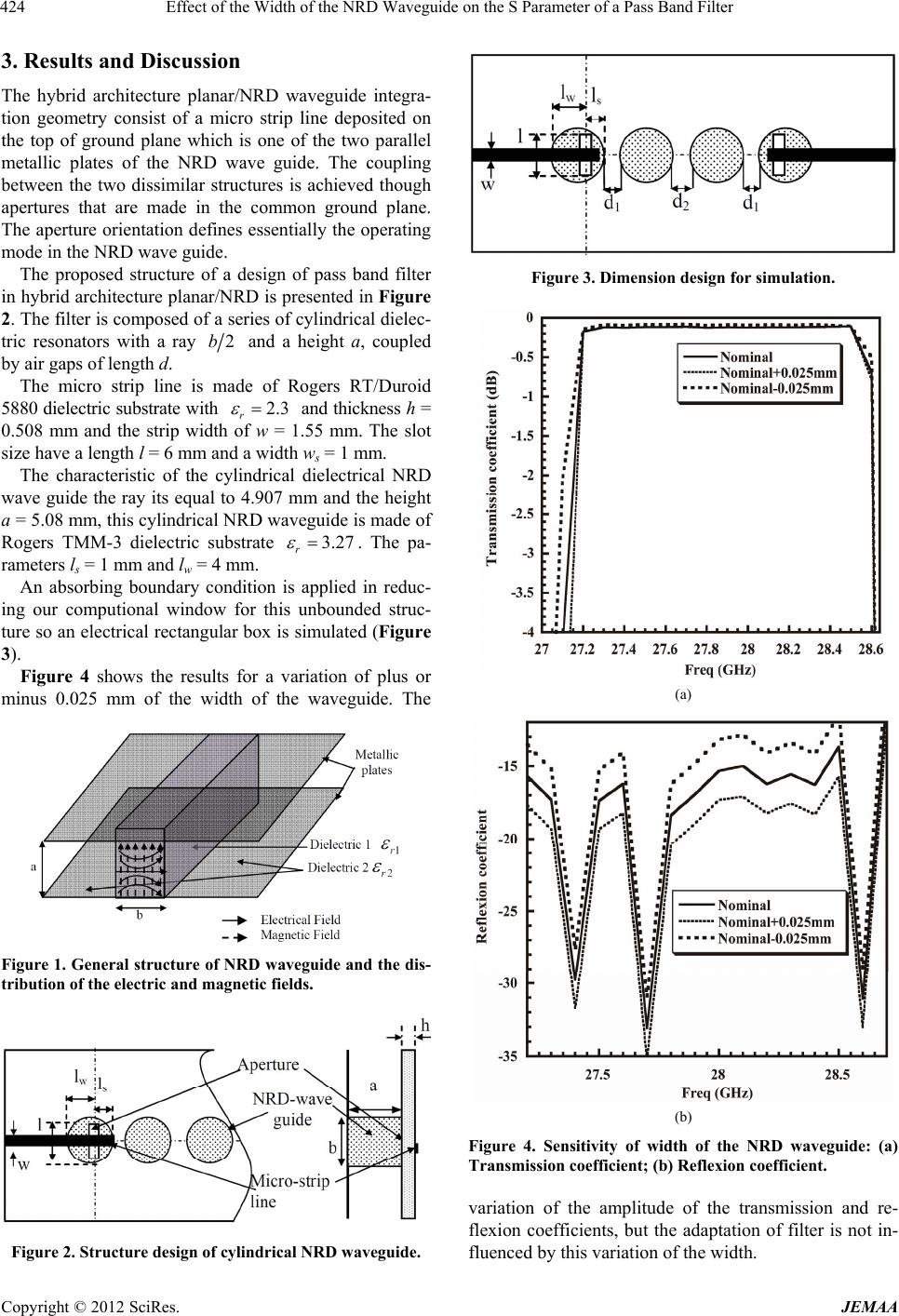 Effect of the Width of the NRD Waveguide on the S Parameter of a Pass Band Filter 424 3. Results and Discussion The hybrid architecture planar/NRD waveguide integra- tion geometry consist of a micro strip line deposited on the top of ground plane which is one of the two parallel metallic plates of the NRD wave guide. The coupling between the two dissimilar structures is achieved though apertures that are made in the common ground plane. The aperture orientation defines essentially the operating mode in the NRD wave guide. The proposed structure of a design of pass band filter in hybrid architecture planar/NRD is presented in Figure 2. The filter is composed of a series of cylindrical dielec- tric resonators with a ray 2b and a height a, coupled by air gaps of length d. The micro strip line is made of Rogers RT/Duroid 5880 dielectric substrate with 2.3 r and thickness h = 0.508 mm and the strip width of w = 1.55 mm. The slot size have a length l = 6 mm and a width ws = 1 mm. The characteristic of the cylindrical dielectrical NRD wave guide the ray its equal to 4.907 mm and the height a = 5.08 mm, this cylindrical NRD waveguide is made of Rogers TMM-3 dielectric substrate 3.27 r . The pa- rameters ls = 1 mm and lw = 4 mm. An absorbing boundary condition is applied in reduc- ing our computional window for this unbounded struc- ture so an electrical rectangular box is simulated (Figure 3). Figure 4 shows the results for a variation of plus or minus 0.025 mm of the width of the waveguide. The Figure 1. General structure of NRD waveguide and the dis- tribution of the electric and magnetic fie lds. Figure 2. Structure design of cylindrical NRD waveguide. Figure 3. Dimension design for simulation. (a) (b) Figure 4. Sensitivity of width of the NRD waveguide: (a) Transmission coefficient; (b) Reflexion coefficient. variation of the amplitude of the transmission and re- flexion coefficients, but the adaptation of filter is not in- fluenced by this variation of the width. Copyright © 2012 SciRes. JEMAA  Effect of the Width of the NRD Waveguide on the S Parameter of a Pass Band Filter Copyright © 2012 SciRes. JEMAA 425 4. Conclusion We have presented the design of pass band filter in hy- brid architecture planar/non radiative dielectric wave guide integration technology and the influence of the va- riation of the width of the NRD waveguide to the pa- rameters S. REFERENCES [1] T. Yoneyama and S. Nishida, “Nonradiative Dielectric Waveguide for Millimeter-Wave Integrated Circuits,” IEEE Transactions on Microwave Theory and Technol- ogy, Vol. 29, No. 11, 1981, pp. 1188-1192. doi:10.1109/TMTT.1981.1130529 [2] T. Yoneyama, “Recent Development in NRD-Guide Tech- nology,” Annales Des Télécommunications, Vol. 47, No. 11-12, 1992, pp. 508-514. [3] T. Yoneyama and S. Nishida, “Non-Radiative Dielectric Waveguide,” In: K. J. Button, Ed., Infrared and Millim- ter Waves Series, 1984, pp. 61-98. [4] A. Bacha and K. Wu “Toward an Optimum Design of NRD-Guide and Microstirp Line Transition for Hybrid Integration Technology,” IEEE Transactions on Micro- Wave Theory and Technology, Vol. 46, No. 11, 1998, pp. 1796-1800. [5] A. Bacha and K. Wu, “LSE -Mode Balun for Hybrid Int e- gration of NRD-Guide and Microstrip Line,” IEEE Mi- cro-Wave and Guided Wave Letters, No. 5, 1998, pp. 199-201. doi:10.1109/75.668729 [6] N. Grigoropoulos and P. R. Young, “Low Cost Non-Ra- diative Perforated Dielectric Waveguide,” Europe Micro- Wave Conference, Munich, 7-9 October 2003, pp. 439- 442. [7] Y. Cassivi and K. Wu, “Substrate Integrated Non-Radia- tive Dielectric Waveguide,” IEEE Micro-Wave Wireless Component Letters, Vol. 14, No. 3, 2004, pp. 89-91. doi:10.1109/LMWC.2004.824808 [8] Y. Cassivi, D. Deslandes and K. Wu, “Engraved NRD- Guide for Millimeter-Wave Integrated Circuits,” IEEE MTT-S International Microwave Symposium Digest, Vol. 2, 2000, pp. 605-608. [9] Y. Cassivi, D. Deslandes and K. Wu, “Design Considera- tions of Engraved NRD-Guide for Millimeter-Wave Inte- grated Circuits,” IEEE Transactions on Microwave The- ory and Technology, Vol. 50, No. 1, 2002, pp. 165-171. doi:10.1109/22.981261 [10] H. Harizi, L. Lattrach and A. Garsallah, “Design of Band Pass Filter in Hybrid Architecture Planar,” American Journal of Applied Science, Vol. 9, No. 10, 2012, pp. 1538-1541. |