

Paper Menu >>
Journal Menu >>
 Materials Sciences and Applications, 2012, 3, 645-649 http://dx.doi.org/10.4236/msa.2012.39094 Published Online September 2012 (http://www.SciRP.org/journal/msa) 645 Preparation of Thin Films by a Bipolar Pulsed-DC Magnetron Sputtering System Using Ca3Co4O9 and CaMnO3 Targets Weerasak Somkhunthot1, Nuwat Pimpabute1, Tosawat Seetawan2 1Program of Physics and Science Center, Faculty of Science and Technology, Loei Rajabhat University, Loei, Thailand; 2Thermoelectrics Research Center, Faculty of Science and Technology, Sakon Nakhon Rajabhat University, Sakon Nakhon, Thailand. Email: [email protected] Received June 7th, 2012; revised July 2nd, 2012; accepted August 5th, 2012 ABSTRACT The thin films were deposited on the glass substrates by an asymmetric bipolar pulsed-dc magnetron sputtering system using the Ca3Co4O9 (p-type) and CaMnO3 (n-type) targets of 60 mm diameter and 2.5 mm thickness. The targets were prepared from powder precursors, which obtained by a solid state reaction. Optical emissions from plasmas during sputter depositions of films were detected using a high resolution spectrometer. Thickness of thin film was estimated by Tolansky’s Fizeau fringe method and ellipsometic measurement. Crystal structures were studied from X-ray diffraction. The thermoelectric properties were assessed from Seebeck coefficient and electrical resistivity measurements at room temperature. The power factors were calculated. It was found that the optical emission spectrums showed that the Ca, Mn, Co and O atoms were sputtered from the targets onto glass substrates. As-deposited Ca-Co-O and Ca-Mn-O films thickness values were 0.435 m and 0.449 m, respectively. The X-ray diffraction patterns clearly showed amorphous nature of the as-deposited films. Determining thermoelectric properties of Ca-Co-O film gave Seebeck coefficient of 0.146 mV/K, electrical resistivity of 0.473 cm, and power factor of 4.531 µW/mK at room temperature. Ca-Mn-O film baring a high resistance was not the experimental determination of thermoelectric properties. Keywords: Thermoelectric Thin Film; Ca3Co4O9; CaMnO3; Bipolar Pulsed-DC Magnetron Sputtering System 1. Introduction In the past, the metal coating in form of thin films to im- prove the quality of material was done by electroplating process which is often also called electro-deposition. The disadvantage of electroplating was harmful to the environ- ment. Subsequently, the vacuum depositions were devel- oped in chemical vapor deposition (CVD) and physical va- por deposition (PVD). CVD is a technique whereby gase- ous reactants can be deposited onto a substrate. However, often dangerous by-products are removed by gas flow. PVD is a clean coating technology that involves evaporation and deposition of a material. Material vaporizes are removed from a source by physical processes such as evaporation sputtering and it is transported in the form of a vapor atomic beam through a vacuum to the substrate. Magnetron sput- tering is one of PVD methods, which are widely used in thin film technology. The various types of magnetron sput- tering technique are direct current (DC), alternating current (AC), radio frequency (RF), and pulsed-dc [1]. Pulsed-dc magnetron sputtering is one of the latest developments of sputtering technology for thin films deposition, which has many advantages over others. Namely, it is versatile and provides the ability to deposit thin films of oxide com- pounds at high deposition rate and to eliminate arcing problems of poisoned targets [2]. This is interested to apply the deposition technology. It may be possible to customize the deposition conditions so that the thin films of highly preferred orientation can be grown. In this work, the depositions of thin films have been car- ried out by a bipolar pulsed-dc magnetron sputtering sys- tem using the Ca3Co4O9 and CaMnO3 targets, which were made from powder precursors obtained from the solid state reaction (SSR) route. Optical emissions from plasmas dur- ing sputter deposition of thin films were measured using a high resolution spectrometer. Crystal structures of the as- deposited films were studied from X-ray diffraction (XRD). The thickness of thin films and thermoelectric properties were investigated. 2. Experimentation The preparation of thin films by a pulsed-dc magnetron sputtering system is shown in Figure 1 [3]. The details of Copyright © 2012 SciRes. MSA 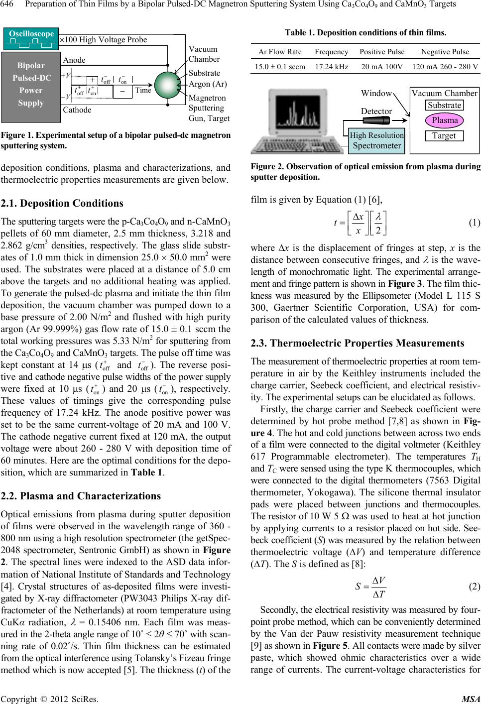 Preparation of Thin Films by a Bipolar Pulsed-DC Magnetron Sputtering System Using Ca3Co4O9 and CaMnO3 Targets 646 on t off t Time Cathode Anode 100 High Voltage Probe Oscilloscope Bipolar Pulsed-DC Power Supply +V V + off t on t Vacuum Chamber Magnetron Sputtering Gun, Target Argon (Ar) Substrate Figure 1. Experimental setup of a bipolar pulsed-dc magnetron sputtering system. deposition conditions, plasma and characterizations, and thermoelectric properties measurements are given below. 2.1. Deposition Conditions The sputtering targets were the p-Ca3Co4O9 and n-CaMnO3 pellets of 60 mm diameter, 2.5 mm thickness, 3.218 and 2.862 g/cm3 densities, respectively. The glass slide substr- ates of 1.0 mm thick in dimension 25.0 50.0 mm2 were used. The substrates were placed at a distance of 5.0 cm above the targets and no additional heating was applied. To generate the pulsed-dc plasma and initiate the thin film deposition, the vacuum chamber was pumped down to a base pressure of 2.00 N/m2 and flushed with high purity argon (Ar 99.999%) gas flow rate of 15.0 ± 0.1 sccm the total working pressures was 5.33 N/m2 for sputtering from the Ca3Co4O9 and CaMnO3 targets. The pulse off time was kept constant at 14 s (off and off t). The reverse posi- tive and cathode negative pulse widths of the power supply were fixed at 10 s (on ) and 20 s (on t), respectively. These values of timings give the corresponding pulse frequency of 17.24 kHz. The anode positive power was set to be the same current-voltage of 20 mA and 100 V. The cathode negative current fixed at 120 mA, the output voltage were about 260 - 280 V with deposition time of 60 minutes. Here are the optimal conditions for the depo- sition, which are summarized in Table 1. t t 2.2. Plasma and Characterizations Optical emissions from plasma during sputter deposition of films were observed in the wavelength range of 360 - 800 nm using a high resolution spectrometer (the getSpec- 2048 spectrometer, Sentronic GmbH) as shown in Figure 2. The spectral lines were indexed to the ASD data infor- mation of National Institute of Standards and Technology [4]. Crystal structures of as-deposited films were investi- gated by X-ray diffractometer (PW3043 Philips X-ray dif- fractometer of the Netherlands) at room temperature using CuKα radiation, = 0.15406 nm. Each film was meas- ured in the 2-theta angle range of 10˚ 2θ 70˚ with scan- ning rate of 0.02˚/s. Thin film thickness can be estimated from the optical interference using Tolansky’s Fizeau fringe method which is now accepted [5]. The thickness (t) of the Table 1. Deposition conditions of thin films. Ar Flow RateFrequency Positive Pulse Negative Pulse sccm kHz mA V mA - V Plasma High Resolution Spectrometer Window DetectorSubstrat e Target Vacuum Chamber Figure 2. Observation of optical emission from plasma during sputter deposition. film is given by Equation (1) [6], 2 x tx (1) where x is the displacement of fringes at step, x is the distance between consecutive fringes, and is the wave- length of monochromatic light. The experimental arrange- ment and fringe pattern is shown in Fi gure 3 . The film thic- kness was measured by the Ellipsometer (Model L 115 S 300, Gaertner Scientific Corporation, USA) for com- parison of the calculated values of thickness. 2.3. Thermoelectric Properties Measurements The measurement of thermoelectric properties at room tem- perature in air by the Keithley instruments included the charge carrier, Seebeck coefficient, and electrical resistiv- ity. The experimental setups can be elucidated as follows. Firstly, the charge carrier and Seebeck coefficient were determined by hot probe method [7,8] as shown in Fig- ure 4. The hot and cold junctions between across two ends of a film were connected to the digital voltmeter (Keithley 617 Programmable electrometer). The temperatures TH and TC were sensed using the type K thermocouples, which were connected to the digital thermometers (7563 Digital thermometer, Yokogawa). The silicone thermal insulator pads were placed between junctions and thermocouples. The resistor of 10 W 5 was used to heat at hot junction by applying currents to a resistor placed on hot side. See- beck coefficient (S) was measured by the relation between thermoelectric voltage (V) and temperature difference (T). The S is defined as [8]: V ST (2) Secondly, the electrical resistivity was measured by four- point probe method, which can be conveniently determined by the Van der Pauw resistivity measurement technique [9] as shown in Figure 5. All contacts were made by silver paste, which showed ohmic characteristics over a wide range of currents. The current-voltage characteristics for Copyright © 2012 SciRes. MSA 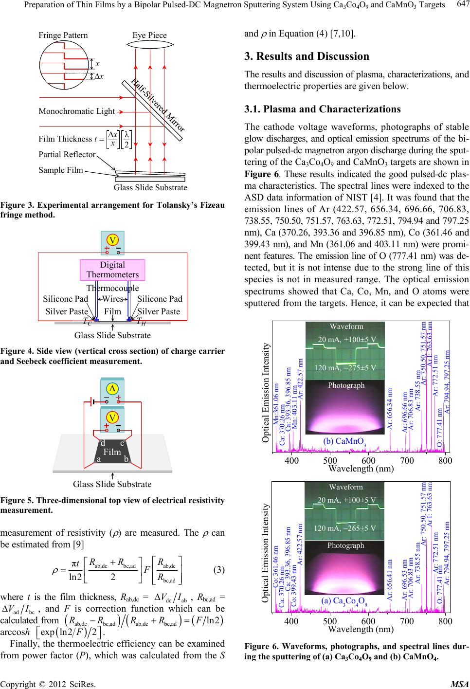 Preparation of Thin Films by a Bipolar Pulsed-DC Magnetron Sputtering System Using Ca3Co4O9 and CaMnO3 Targets 647 Glass Slide Substrate x x Monochromatic Light Eye Piece Fringe Pattern Partial Reflector Film Thickness t x x 2 = Sample Film Figure 3. Experimental arrangement for Tolansky’s Fizeau fringe method. Film Silver Paste Silicone Pad Thermocouple Wires Glass Slide Substrate Silver Paste Silicone Pad V Digital Thermo met ers T C T H Figure 4. Side view (vertical cross section) of charge carrier and Seebeck coefficient measurement. Glass Slide Substrate Film a b c d V A Figure 5. Thre e-dime nsional top view of elec tric al re sistiv ity measurement. measurement of resistivity ( ) are measured. The can be estimated from [9] ab,dc bc,adab,dc b c,ad π ln2 2 RR R tFR (3) where t is the film thickness, Rab,dc = dc ab VI, Rbc,ad = ad bc VI, and F is correction function which can be calculated from ab,dc bc,adab,dc bc,adln2RR RRF arccosh exp ln22F . Finally, the thermoelectric efficiency can be examined from power factor (P), which was calculated from the S and in Equation (4) [7,10]. 3. Results and Discussion The results and discussion of plasma, characterizations, and thermoelectric properties are given below. 3.1. Plasma and Characterizations The cathode voltage waveforms, photographs of stable glow discharges, and optical emission spectrums of the bi- polar pulsed-dc magnetron argon discharge during the sput- tering of the Ca3Co4O9 and CaMnO3 targets are shown in Figure 6. These results indicated the good pulsed-dc plas- ma characteristics. The spectral lines were indexed to the ASD data information of NIST [4]. It was found that the emission lines of Ar (422.57, 656.34, 696.66, 706.83, 738.55, 750.50, 751.57, 763.63, 772.51, 794.94 and 797.25 nm), Ca (370.26, 393.36 and 396.85 nm), Co (361.46 and 399.43 nm), and Mn (361.06 and 403.11 nm) were promi- nent features. The emission line of O (777.41 nm) was de- tected, but it is not intense due to the strong line of this species is not in measured range. The optical emission spectrums showed that Ca, Co, Mn, and O atoms were sputtered from the targets. Hence, it can be expected that 400 500 600700 800 (b) CaMnO3 Ar: 696.66 nm Mn: 403.11 nm O: 777.41 nm Ar: 794.94, 797.25 nm Ar: 772.51 nm Ar I: 763.63 nm Ar: 750.50, 751.57 nm Ar: 738.55 nm Ar: 706.83 nm Ar: 656.34 nm Ar: 422.57 nm Ca: 393.36, 396.85 nm Ca: 370.26 nm Mn:361.06 nm Optical Emission Intensity Wavelength (nm) 20 mA, +100±5 V 120 mA, 275±5 V Waveform Photograph 400 500 600700 800 (a) Ca3Co4O9 Ar: 696.53 nm Co: 399.43 nm O: 777.41 nm Ar: 794.94, 797.25 nm Ar: 772.51 nmAr I: 763.63 nm Ar: 750.50, 751.57 nm Ar: 738.55 nm Ar: 706.83 nm Ar: 656.41 nm Ar: 422.57 nm Ca: 393.36, 396.85 nm Ca: 370.26 nm Co: 361.46 nm Optical Emission Intensity Wavelength (nm) Waveform 20 mA, +100±5 V 120 mA, 265±5 V Photograph Figure 6. Waveforms, photographs, and spectral lines dur- ing the sputtering of (a) Ca3Co4O9 and (b) CaMnO4. Copyright © 2012 SciRes. MSA 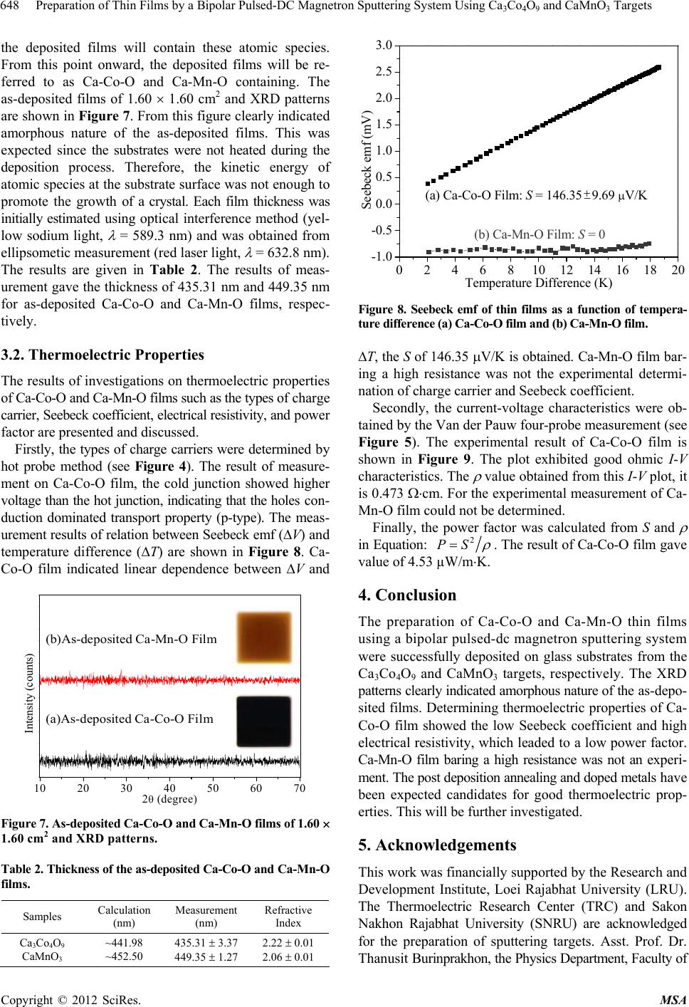 Preparation of Thin Films by a Bipolar Pulsed-DC Magnetron Sputtering System Using Ca3Co4O9 and CaMnO3 Targets 648 the deposited films will contain these atomic species. From this point onward, the deposited films will be re- ferred to as Ca-Co-O and Ca-Mn-O containing. The as-deposited films of 1.60 1.60 cm2 and XRD patterns are shown in Figure 7. From this figure clearly indicated amorphous nature of the as-deposited films. This was expected since the substrates were not heated during the deposition process. Therefore, the kinetic energy of atomic species at the substrate surface was not enough to promote the growth of a crystal. Each film thickness was initially estimated using optical interference method (yel- low sodium light, = 589.3 nm) and was obtained from ellipsometic measurement (red laser light, = 632.8 nm). The results are given in Table 2. The results of meas- urement gave the thickness of 435.31 nm and 449.35 nm for as-deposited Ca-Co-O and Ca-Mn-O films, respec- tively. 3.2. Thermoelectric Properties The results of investigations on thermoelectric properties of Ca-Co-O and Ca-Mn-O films such as the types of charge carrier, Seebeck coefficient, electrical resistivity, and power factor are presented and discussed. Firstly, the types of charge carriers were determined by hot probe method (see Figure 4). The result of measure- ment on Ca-Co-O film, the cold junction showed higher voltage than the hot junction, indicating that the holes con- duction dominated transport property (p-type). The meas- urement results of relation between Seebeck emf (V) and temperature difference (T) are shown in Figure 8. Ca- Co-O film indicated linear dependence between V and 10 20 30 40 50 60 70 Intensity (counts) 2 (degree) (a) As-deposted Ca-Co-O Film (a) As-deposted Ca-Mn-O Film (b) As-deposited Ca-Mn-O Film (a) As-deposited Ca-Co-O Film (b)As-deposited Ca-Mn-O Film (a)As-deposited Ca-Co-O Film Figure 7. As-deposited Ca-Co-O and Ca-Mn-O films of 1.60 1.60 cm2 and XRD patterns. Table 2. Thickness of the as-deposited Ca-Co-O and Ca- M n- O films. Samples Calculation (nm) Measurement (nm) Refractive Index Ca3Co4O9 CaMnO3 ~441.98 ~452.50 435.31 3.37 449.35 1.27 2.22 0.01 2.06 0.01 024681012 14 16 18 20 -1.0 -0.5 0.0 0.5 1.0 1.5 2.0 2.5 3.0 (b) Ca-Mn-O Film: S = 0 (a) Ca-Co-O Film: S = 146.35 9.69 V/K Seebeck emf (mV) Temperature Difference (K) Figure 8. Seebeck emf of thin films as a function of tempera- ture difference (a) Ca-C o-O film and (b) C a-Mn-O film. T, the S of 146.35 V/K is obtained. Ca-Mn-O film bar- ing a high resistance was not the experimental determi- nation of charge carrier and Seebeck coefficient. Secondly, the current-voltage characteristics were ob- tained by the Van der Pauw four-probe measurement (see Figure 5). The experimental result of Ca-Co-O film is shown in Figure 9. The plot exhibited good ohmic I-V characteristics. The value obtained from this I-V plot, it is 0.473 cm. For the experimental measurement of Ca- Mn-O film could not be determined. Finally, the power factor was calculated from S and in Equation: 2 PS . The result of Ca-Co-O film gave value of 4.53 µW/mK. 4. Conclusion The preparation of Ca-Co-O and Ca-Mn-O thin films using a bipolar pulsed-dc magnetron sputtering system were successfully deposited on glass substrates from the Ca3Co4O9 and CaMnO3 targets, respectively. The XRD patterns clearly indicated amorphous nature of the as-depo- sited films. Determining thermoelectric properties of Ca- Co-O film showed the low Seebeck coefficient and high electrical resistivity, which leaded to a low power factor. Ca-Mn-O film baring a high resistance was not an experi- ment. The post deposition annealing and doped metals have been expected candidates for good thermoelectric prop- erties. This will be further investigated. 5. Acknowledgements This work was financially supported by the Research and Development Institute, Loei Rajabhat University (LRU). The Thermoelectric Research Center (TRC) and Sakon Nakhon Rajabhat University (SNRU) are acknowledged for the preparation of sputtering targets. Asst. Prof. Dr. Thanusit Burinprakhon, the Physics Department, Faculty of Copyright © 2012 SciRes. MSA 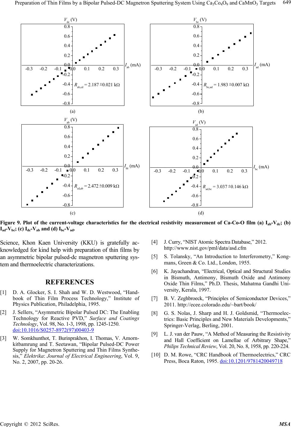 Preparation of Thin Films by a Bipolar Pulsed-DC Magnetron Sputtering System Using Ca3Co4O9 and CaMnO3 Targets Copyright © 2012 SciRes. MSA 649 -0.3-0.2-0.10.0 0.1 0.2 0.3 -0.8 -0.6 -0.4 -0.2 0.0 0.2 0.4 0.6 0.8 Rab,cd = 2.187 0.021 k V dc (V) Iab (mA) (a) -0.3-0.2-0.10.0 0.1 0.2 0.3 -0.8 -0.6 -0.4 -0.2 0.0 0.2 0.4 0.6 0.8 Rbc,ad = 1.983 0.007 k V bc (V) Iad (mA) (b) (a) (b) -0.3-0.2-0.10.0 0.1 0.2 0.3 -0.8 -0.6 -0.4 -0.2 0.0 0.2 0.4 0.6 0.8 Rcd,ab = 2.472 0.009 k V ab (V) Idc (mA) (c) -0.3-0.2-0.10.00.1 0.2 0.3 -0.8 -0.6 -0.4 -0.2 0.0 0.2 0.4 0.6 0.8 Rad,bc = 3.037 0.146 k V ad (V) Ibc (mA) (d) (c) (d) Figure 9. Plot of the current-voltage characteristics for the electrical resistivity measurement of Ca-Co-O film (a) Iab-Vdc; (b) Iad-Vbc; (c) Idc-Vab and (d) Ibc-Vad. [4] J. Curry, “NIST Atomic Spectra Database,” 2012. http://www.nist.gov/pml/data/asd.cfm Science, Khon Kaen University (KKU) is gratefully ac- knowledged for kind help with preparation of thin films by an asymmetric bipolar pulsed-dc magnetron sputtering sys- tem and thermoelectric characterizations. [5] S. Tolansky, “An Introduction to Interferometry,” Kong- mans, Green & Co. Ltd., London, 1955. [6] K. Jayachandran, “Electrical, Optical and Structural Studies in Bismuth, Antimony, Bismuth Oxide and Antimony Oxide Thin Films,” Ph.D. Thesis, Mahatma Gandhi Uni- versity, Kerala, 1997. REFERENCES [1] D. A. Glocker, S. I. Shah and W. D. Westwood, “Hand- book of Thin Film Process Technology,” Institute of Physics Publication, Philadelphia, 1995. [7] B. V. Zeghbroeck, “Principles of Semiconductor Devices,” 2011. http://ecee.colorado.edu/~bart/book/ [2] J. Sellers, “Asymmetric Bipolar Pulsed DC: The Enabling Technology for Reactive PVD,” Surface and Coatings Technology, Vol. 98, No. 1-3, 1998, pp. 1245-1250. doi:10.1016/S0257-8972(97)00403-9 [8] G. S. Nolas, J. Sharp and H. J. Goldsmid, “Thermoelec- trics: Basic Principles and New Materials Developments,” Springer-Verlag, Berling, 2001. [9] L. J. van der Pauw, “A Method of Measuring the Resistivity and Hall Coefficient on Lamellae of Arbitrary Shape,” Philips Technical Review, Vol. 20, No. 8, 1958, pp. 220-224. [3] W. Somkhunthot, T. Burinprakhon, I. Thomas, V. Amorn- kitbamrung and T. Seetawan, “Bipolar Pulsed-DC Power Supply for Magnetron Sputtering and Thin Films Synthe- sis,” Elektrika: Journal of Electrical Engineering, Vol. 9, No. 2, 2007, pp. 20-26. [10] D. M. Rowe, “CRC Handbook of Thermoelectrics,” CRC Press, Boca Raton, 1995. doi:10.1201/9781420049718 |