

Paper Menu >>
Journal Menu >>
 World Journal of Nano Science and Engineering, 2012, 2, 88-91 http://dx.doi.org/10.4236/wjnse.2012.22011 Published Online June 2012 (http://www.SciRP.org/journal/wjnse) Design Consideration in the Development of Multi-Fin FETs for RF Applications Peijie Feng, Prasanta Ghosh Department of Electrical Engineering and Computer Science, Syracuse University, Syracuse, USA Email: [email protected] Received March 7, 2012; revised April 17, 2012; accepted May 16, 2012 ABSTRACT In this paper, we propose multi-fin FET design techniques targeted for RF applications. Overlap and underlap design configuration in a base FinFET are compared first and then multi-fin device (consisting of transistor unit up to 50) is studied to develop design limitations and to evaluate their effects on the device performance. We have also investigated the impact of the number of fins (up to 50) in multi-fin structure and resulting RF parameters. Our results show that as the number of fin increases, underlap design compromises RF performance and short channel effects. The results pro- vide technical understanding that is necessary to realize new opportunities for RF and analog mixed-signal design with nanoscale FinFETs. Keywords: FinFET; Analog; RF; Source/Drain Extension Region Engineering; Simulation; Multi-Fin FET 1. Introduction According to the International Technology Roadmap for Semiconductors (ITRS), as transistor dimension scaling into nanometer regime, the conventional planar bulk MOSFET technology faces many challenges: e.g., the close proximity between source and drain worsens leak- age current; the necessary high doping in the bulk causes threshold voltage fluctuation, etc. [1]. FinFET, emerging as a promising device, addresses those Short Channel Effects (SCEs) and secures the necessary performance in the sub-32 nm regime due to its scalability, superior SCEs, and compatibilities to the planar CMOS platform. Our survey reveals that recent papers are more on Fin- FET’s digital application and less on analog/RF figures of merit (FoM) [2]. Several papers present work on source/ drain extension (SDE) region engineering with the goal of improving a single-fin FET or coupling FinFETs per- formance (NFinFET ≤ 5) [3-5]. Only few papers are on ana- log/RF FoM of multi-fin FETs which introduces a large total channel width to achieve high transconductance, maintain good noise and mismatch performance [2]. In this paper, with extensive calibrated TCAD simula- tions, we present results for SCEs and analog/RF FoM of a base FinFET unit and then a multi-fin FET (NFinFET up to 50). The effect of SDE engineering on the multi-fin device RF performance is studied. Simulations along with theoretical analysis establish the realistic application potential of underlap design for the multi-Fin FET RF operation. 2. Simulation Setup and Results 2.1. Base FinFET Unit Given that base FinFET units within the multi-fin config- uration are nominal identical to each other, we first optimize analog/RF FoM of a 22 nm node single-fin FET which then will be used as a base transistor for a multi- fin structure [6]. The gate length (Lg) of the n-type FinFET is set at 25 nm. The fin height (Hfin) is fixed at 50 nm. The bulk is lightly doped 1015 cm–3 to avoid the dopant fluctuation. Selective epitaxial growth with heavy doping are performed for the source/drain region to minimize the parasitic resistance. SDE region engineering is con- sidered by the application of overlap and underlap design. Abrupt junction, which is achievable by solid re-growth and laser annealing process [5], is designed with a fast doping decay with lateral straggle (σS/D) at the value of 1 nm/dev at the edge of SDE region whereas the underlap doping profile in the SDE region is simulated with a Gaussian model rolling off from a peak value of 1020 cm–3 at the edge of the source/drain. The equivalent oxide thickness (EOT) of the Hf-based dielectric in the simulation is 0.7 nm. The work-function of the TiN metal gate is adjusted to 4.6 eV such that the threshold voltage Vt of the device is around 0.3 V. The device is investi- gated with a calibrated TCAD simulation taking into account quantum effect with Lombardi mobility model [7]. The design of TCAD experiments shown in Table 1 for this study considers the trade-off between current drivability and SCEs. Overlap design enhances current C opyright © 2012 SciRes. WJNSE 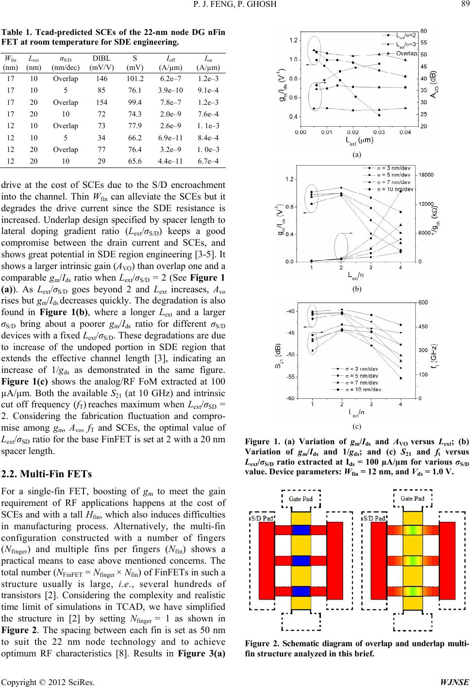 P. J. FENG, P. GHOSH 89 Table 1. Tcad-predicted SCEs of the 22-nm node DG nFin FET at room tempe r a ture for SDE en g i neering. Wfin (nm) Lext (nm) σS/D (nm/dec) DIBL (mV/V) S (mV) Ioff (A/µm) Ion (A/µm) 17 10 Overlap 146 101.2 6.2e–7 1.2e–3 17 10 5 85 76.1 3.9e–10 9.1e–4 17 20 Overlap 154 99.4 7.8e–7 1.2e–3 17 20 10 72 74.3 2.0e–9 7.6e–4 12 10 Overlap 73 77.9 2.6e–9 1. 1e–3 12 10 5 34 66.2 6.9e–11 8.4e–4 12 20 Overlap 77 76.4 3.2e–9 1. 0e–3 12 20 10 29 65.6 4.4e–11 6.7e–4 drive at the cost of SCEs due to the S/D encroachment into the channel. Thin Wfin can alleviate the SCEs but it degrades the drive current since the SDE resistance is increased. Underlap design specified by spacer length to lateral doping gradient ratio (Lext/σS/D) keeps a good compromise between the drain current and SCEs, and shows great potential in SDE region engineering [3-5]. It shows a larger intrinsic gain (AVO) than overlap one and a comparable gm/Ids ratio when Lext/σS/D = 2 (See Figure 1 (a)). As Lext/σS/D goes beyond 2 and Lext increases, Avo rises but gm/Ids decreases quickly. The degradation is also found in Figure 1(b), where a longer Lext and a larger σS/D bring about a poorer gm/Ids ratio for different σS/D devices with a fixed Lext/σS/D. These degradations are due to increase of the undoped portion in SDE region that extends the effective channel length [3], indicating an increase of 1/gds as demonstrated in the same figure. Figure 1(c) shows the analog/RF FoM extracted at 100 µA/µm. Both the available S21 (at 10 GHz) and intrinsic cut off frequency (fT) reaches maximum when Lext/σSD = 2. Considering the fabrication fluctuation and compro- mise among gm, Avo, fT and SCEs, the optimal value of Lext/σSD ratio for the base FinFET is set at 2 with a 20 nm spacer length. 2.2. Multi-Fin FETs For a single-fin FET, boosting of gm to meet the gain requirement of RF applications happens at the cost of SCEs and with a tall Hfin, which also induces difficulties in manufacturing process. Alternatively, the multi-fin configuration constructed with a number of fingers (Nfinger) and multiple fins per fingers (Nfin) shows a practical means to ease above mentioned concerns. The total number (NFinFET = Nfinger × Nfin) of FinFETs in such a structure usually is large, i.e., several hundreds of transistors [2]. Considering the complexity and realistic time limit of simulations in TCAD, we have simplified the structure in [2] by setting Nfinger = 1 as shown in Figure 2. The spacing between each fin is set as 50 nm to suit the 22 nm node technology and to achieve optimum RF characteristics [8]. Results in Figure 3(a) (a) (b) (c) Figure 1. (a) Variation of gm/Ids and AVO versus Lext; (b) Variation of gm/Ids and 1/gds; and (c) S21 and ft versus Lext/σS/D ratio extracted at Ids = 100 µA/µm for various σS/D value. Device parameters: Wfin = 12 nm, and Vds = 1.0 V. Figure 2. Schematic diagram of overlap and underlap multi- fin structure analyzed in this brief. Copyright © 2012 SciRes. WJNSE 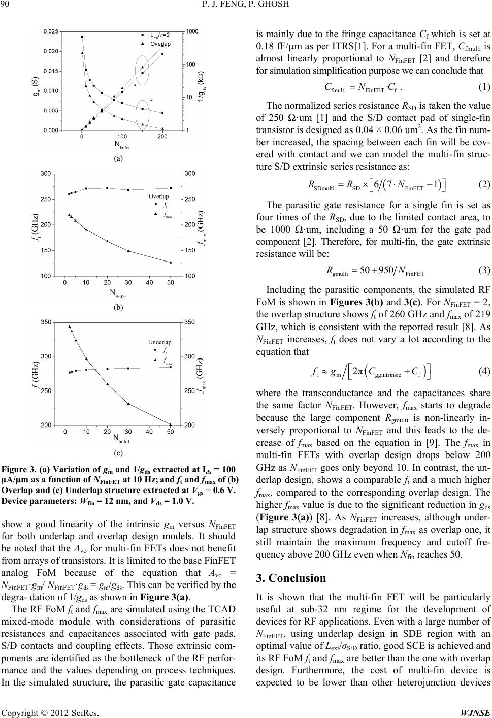 P. J. FENG, P. GHOSH 90 (a) (b) (c) Figure 3. (a) Variation of gm and 1/gds extracted at Ids = 100 µA/µm as a function of NFinFET at 10 Hz; and ft and fmax of (b) Overlap and (c) Underlap structure extracted at Vgs = 0.6 V. Device parameters: Wfin = 12 nm, and Vds = 1.0 V. show a good linearity of the intrinsic gm versus NFinFET for both underlap and overlap design models. It should be noted that the Avo for multi-fin FETs does not benefit from arrays of transistors. It is limited to the base FinFET analog FoM because of the equation that Avo = NFinFET·gm/ NFinFET·gds = gm/gds. This can be verified by the degra- dation of 1/gds as shown in Fi g ure 3( a). The RF FoM ft and fmax are simulated using the TCAD mixed-mode module with considerations of parasitic resistances and capacitances associated with gate pads, S/D contacts and coupling effects. Those extrinsic com- ponents are identified as the bottleneck of the RF perfor- mance and the values depending on process techniques. In the simulated structure, the parasitic gate capacitance is mainly due to the fringe capacitance Cf which is set at 0.18 fF/µm as per ITRS[1]. For a multi-fin FET, Cfmulti is almost linearly proportional to NFinFET [2] and therefore for simulation simplification purpose we can conclude that fmultiFinFET f ·CNC . (1) The normalized series resistance RSD is taken the value of 250 Ω·um [1] and the S/D contact pad of single-fin transistor is designed as 0.04 × 0.06 um2. As the fin num- ber increased, the spacing between each fin will be cov- ered with contact and we can model the multi-fin struc- ture S/D extrinsic series resistance as: SDmulti SDFinFET 67 1RR N (2) The parasitic gate resistance for a single fin is set as four times of the RSD, due to the limited contact area, to be 1000 Ω·um, including a 50 Ω·um for the gate pad component [2]. Therefore, for multi-fin, the gate extrinsic resistance will be: gmulti FinFET 50 950RN (3) Including the parasitic components, the simulated RF FoM is shown in Figures 3(b) and 3(c). For NFinFET = 2, the overlap structure shows ft of 260 GHz and fmax of 219 GHz, which is consistent with the reported result [8]. As NFinFET increases, ft does not vary a lot according to the equation that tmggintrinsic f 2π·fg CC (4) where the transconductance and the capacitances share the same factor NFinFET. However, fmax starts to degrade because the large component Rgmulti is non-linearly in- versely proportional to NFinFET and this leads to the de- crease of fmax based on the equation in [9]. The fmax in multi-fin FETs with overlap design drops below 200 GHz as NFinFET goes only beyond 10. In contrast, the un- derlap design, shows a comparable ft and a much higher fmax, compared to the corresponding overlap design. The higher fmax value is due to the significant reduction in gds (Figure 3(a)) [8]. As NFinFET increases, although under- lap structure shows degradation in fmax as overlap one, it still maintain the maximum frequency and cutoff fre- quency above 200 GHz even when Nfin reaches 50. 3. Conclusion It is shown that the multi-fin FET will be particularly useful at sub-32 nm regime for the development of devices for RF applications. Even with a large number of NFinFET, using underlap design in SDE region with an optimal value of Lext/σS/D ratio, good SCE is achieved and its RF FoM ft and fmax are better than the one with overlap design. Furthermore, the cost of multi-fin device is expected to be lower than other heterojunction devices Copyright © 2012 SciRes. WJNSE  P. J. FENG, P. GHOSH Copyright © 2012 SciRes. WJNSE 91 and III-V compound devices because of its compatibility with the CMOS planar process technology. 4. Acknowledgements The authors would like to thank Synopsys, Inc., for pro- viding the Sentaurus TCAD tool set for device design and simulation. REFERENCES [1] “International Technology Roadmap for Semiconductors,” 2011. http://www.public.itrs.net [2] V. Subramanian, A. Mercha, B. Parvais, M. Dehan, G. Groeseneken, W. Sansen and S. Decoutere, “Identifying the Bottlenecks to the RF Performance of FinFETs,” Proceedings of the 23rd Annual International Conference on VLSI Design, Bangalore, 3-7 January 2010, pp. 111-116. [3] V. Trivedi, J. G. Fossum and M. M. Chowdhury, “Nano- scale FinFETs with Gate-Source/Drain Underlap,” IEEE Transactions on Electron Devices, Vol. 52, No. 1, 2005, pp. 56-62. doi:10.1109/TED.2004.841333 [4] A. Kranti and G. M. Armstrong, “Design and Optimiza- tion of FinFETs for Ultra-Low-Voltage Analog Applica- tions,” IEEE Transactions on Electron Devices, Vol. 54, No. 12, 2007, pp. 3308-3316. doi:10.1109/TED.2007.908596 [5] J. Yang, P. M. Zeitzoff and H. Tseng, “Highly Manufac- turable Double-Gate FinFET With Gate-Source/Drain Un- derlap,” IEEE Transactions on Electron Devices, Vol. 54, No. 6, 2007, pp. 1464-1470. doi:10.1109/TED.2007.896387 [6] P. Feng and P. K. Ghosh, “Comparison of Silicon-on- Insulator and Body-on-Insulator FinFET Based Digital Circuits with Consideration on Self-Heating Effects,” IEEE International Semiconductor Device Research Sym- posium, College Park, Maryland, 7-9 December 2010, pp. 1-2. [7] “Sentaurus Device Manual,” Synopsys, Santa Clara, 2010. [8] A. Kranti, J. Raskin and G. A. Armstrong, “Optimizing FinFET Geometry and Parasitics for RF Applications,” Proceedings of the IEEE International SOI Conference, New Paltz, New York, 6-9 Octorber 2008, pp. 123-124. [9] J.-P. Raskin, G. Pailloncy, D. Lederer, F. Danneville, G. Dambrine, S. Decoutere, A. Mercha and B. Parvais, “High- Frequency Noise Performance of 60-nm Gate-Length Fin- FETs,” IEEE Transactions on Electron Devices, Vol. 55, No. 10, 2008, pp. 2718-2727. doi:10.1109/TED.2008.2003097 |