

Paper Menu >>
Journal Menu >>
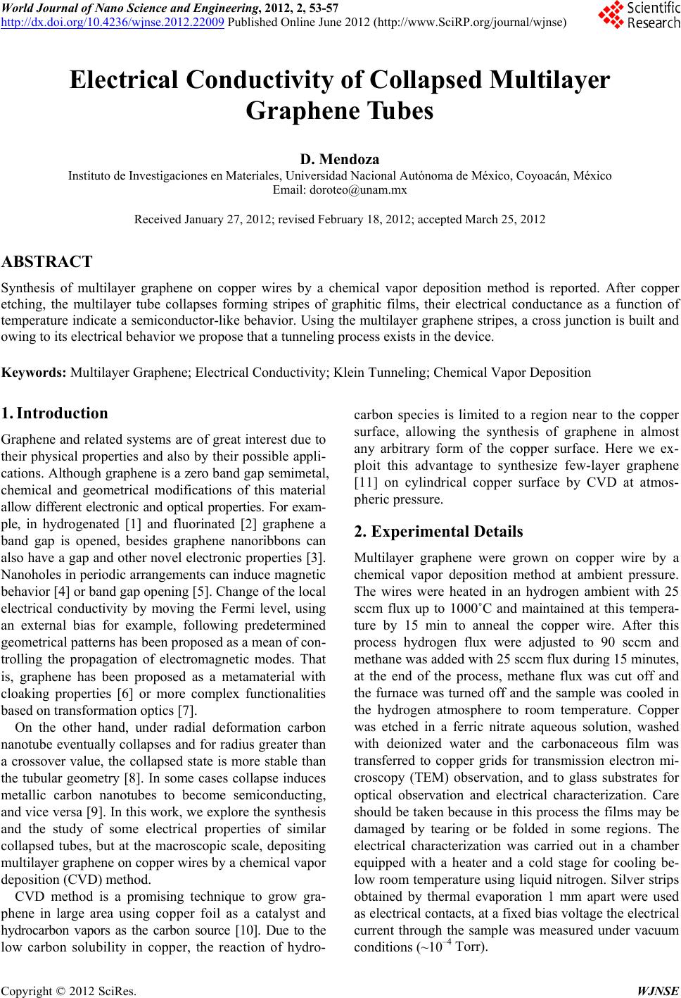 World Journal of Nano Science and Engineering, 2012, 2, 53-57 http://dx.doi.org/10.4236/wjnse.2012.22009 Published Online June 2012 (http://www.SciRP.org/journal/wjnse) Electrical Conductivity of Collapsed Multilayer Graphene Tubes D. Mendoza Instituto de Investigaciones en Materiales, Universidad Nacional Autónoma de México, Coyoacán, México Email: [email protected] Received January 27, 2012; revised February 18, 2012; accepted March 25, 2012 ABSTRACT Synthesis of multilayer graphene on copper wires by a chemical vapor deposition method is reported. After copper etching, the multilayer tube collapses forming stripes of graphitic films, their electrical conductance as a function of temperature indicate a semiconductor-like behavior. Using the multilayer graphene stripes, a cross junction is built and owing to its electrical behavior we propose that a tunneling process exists in the device. Keywords: Multilayer Graphene; Electrical Conductivity; Klein Tunneling; Chemical Vapor Deposition 1. Introduction Graphene and related systems are of great interest due to their physical properties and also by their possible appli- cations. Although graphene is a zero band gap semimetal, chemical and geometrical modifications of this material allow different electronic and optical properties. For exam- ple, in hydrogenated [1] and fluorinated [2] graphene a band gap is opened, besides graphene nanoribbons can also have a gap and other novel electronic properties [3]. Nanoholes in periodic arrangements can induce magnetic behavior [4] or band gap opening [5]. Change of the local electrical conductivity by moving the Fermi level, using an external bias for example, following predetermined geometrical patterns has been proposed as a mean of con- trolling the propagation of electromagnetic modes. That is, graphene has been proposed as a metamaterial with cloaking properties [6] or more complex functionalities based on transformation optics [7]. On the other hand, under radial deformation carbon nanotube eventually collapses and for radius greater than a crossover value, the collapsed state is more stable than the tubular geometry [8]. In some cases collapse induces metallic carbon nanotubes to become semiconducting, and vice versa [9]. In this work, we explore the synthesis and the study of some electrical properties of similar collapsed tubes, but at the macroscopic scale, depositing multilayer graphene on copper wires by a chemical vapor deposition (CVD) method. CVD method is a promising technique to grow gra- phene in large area using copper foil as a catalyst and hydrocarbon vapors as the carbon source [10]. Due to the low carbon solubility in copper, the reaction of hydro- carbon species is limited to a region near to the copper surface, allowing the synthesis of graphene in almost any arbitrary form of the copper surface. Here we ex- ploit this advantage to synthesize few-layer graphene [11] on cylindrical copper surface by CVD at atmos- pheric pressure. 2. Experimental Details Multilayer graphene were grown on copper wire by a chemical vapor deposition method at ambient pressure. The wires were heated in an hydrogen ambient with 25 sccm flux up to 1000˚C and maintained at this tempera- ture by 15 min to anneal the copper wire. After this process hydrogen flux were adjusted to 90 sccm and methane was added with 25 sccm flux during 15 minutes, at the end of the process, methane flux was cut off and the furnace was turned off and the sample was cooled in the hydrogen atmosphere to room temperature. Copper was etched in a ferric nitrate aqueous solution, washed with deionized water and the carbonaceous film was transferred to copper grids for transmission electron mi- croscopy (TEM) observation, and to glass substrates for optical observation and electrical characterization. Care should be taken because in this process the films may be damaged by tearing or be folded in some regions. The electrical characterization was carried out in a chamber equipped with a heater and a cold stage for cooling be- low room temperature using liquid nitrogen. Silver strips obtained by thermal evaporation 1 mm apart were used as electrical contacts, at a fixed bias voltage the electrical current through the sample was measured under vacuum conditions (~10–4 Torr). C opyright © 2012 SciRes. WJNSE 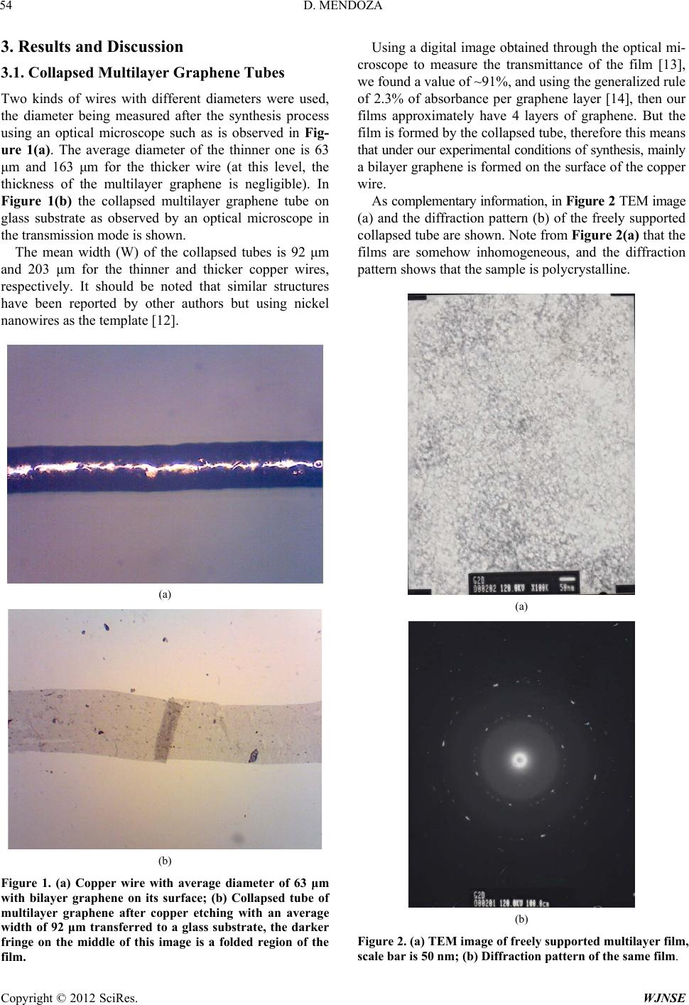 D. MENDOZA 54 3. Results and Discussion 3.1. Collapsed Multilayer Graphene Tubes Two kinds of wires with different diameters were used, the diameter being measured after the synthesis process using an optical microscope such as is observed in Fig- ure 1(a). The average diameter of the thinner one is 63 μm and 163 μm for the thicker wire (at this level, the thickness of the multilayer graphene is negligible). In Figure 1(b) the collapsed multilayer graphene tube on glass substrate as observed by an optical microscope in the transmission mode is shown. The mean width (W) of the collapsed tubes is 92 μm and 203 μm for the thinner and thicker copper wires, respectively. It should be noted that similar structures have been reported by other authors but using nickel nanowires as the template [12]. (a) (b) Figure 1. (a) Copper wire with average diameter of 63 μm with bilayer graphene on its surface; (b) Collapsed tube of multilayer graphene after copper etching with an average width of 92 μm transferred to a glass substrate, the darker fringe on the middle of this image is a folded region of the film. Using a digital image obtained through the optical mi- croscope to measure the transmittance of the film [13], we found a value of ~91%, and using the generalized rule of 2.3% of absorbance per graphene layer [14], then our films approximately have 4 layers of graphene. But the film is formed by the collapsed tube, therefore this means that under our experimental conditions of synthesis, mainly a bilayer graphene is formed on the surface of the copper wire. As complementary information, in Figure 2 TEM image (a) and the diffraction pattern (b) of the freely supported collapsed tube are shown. Note from Figure 2(a) that the films are somehow inhomogeneous, and the diffraction pattern shows that the sample is polycrystalline. (a) (b) Figure 2. (a) TEM image of freely supported multilayer film, scale bar is 50 nm; (b) Diffraction pattern of the same film. Copyright © 2012 SciRes. WJNSE 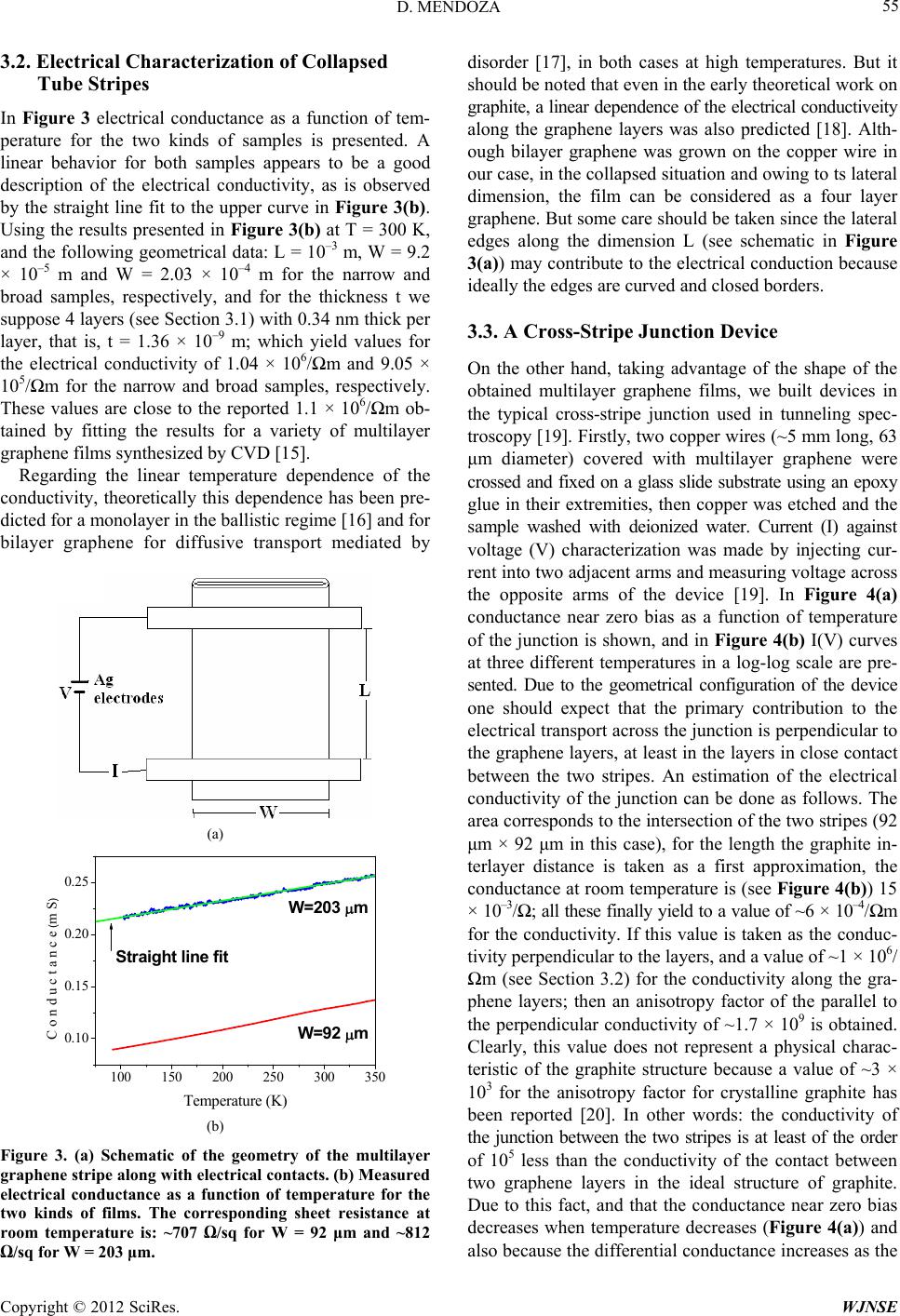 D. MENDOZA 55 3.2. Electrical Characterization of Collapsed Tube Stripes In Figure 3 electrical conductance as a function of tem- perature for the two kinds of samples is presented. A linear behavior for both samples appears to be a good description of the electrical conductivity, as is observed by the straight line fit to the upper curve in Figure 3(b). Using the results presented in Figure 3(b) at T = 300 K, and the following geometrical data: L = 10–3 m, W = 9.2 × 10⁻⁵ m and W = 2.03 × 10⁻⁴ m for the narrow and broad samples, respectively, and for the thickness t we suppose 4 layers (see Section 3.1) with 0.34 nm thick per layer, that is, t = 1.36 × 10⁻⁹ m; which yield values for the electrical conductivity of 1.04 × 10⁶/Ωm and 9.05 × 10⁵/Ωm for the narrow and broad samples, respectively. These values are close to the reported 1.1 × 10⁶/Ωm ob- tained by fitting the results for a variety of multilayer graphene films synthesized by CVD [15]. Regarding the linear temperature dependence of the conductivity, theoretically this dependence has been pre- dicted for a monolayer in the ballistic regime [16] and for bilayer graphene for diffusive transport mediated by (a) 100 150 200 250 300 350 0.10 0.15 0.20 0.25 C o n d u c t a n c e (m S) Temperature (K) W=203 m W=92 m Stra ig h t lin e fit (b) (b) Figure 3. (a) Schematic of the geometry of the multilayer graphene stripe along with electrical contacts. (b) Measured electrical conductance as a function of temperature for the two kinds of films. The corresponding sheet resistance at room temperature is: ~707 Ω/sq for W = 92 μm and ~812 Ω/sq for W = 203 μm. disorder [17], in both cases at high temperatures. But it should be noted that even in the early theoretical work on graphite, a linear dependence of the electrical conductiveity along the graphene layers was also predicted [18]. Alth- ough bilayer graphene was grown on the copper wire in our case, in the collapsed situation and owing to ts lateral dimension, the film can be considered as a four layer graphene. But some care should be taken since the lateral edges along the dimension L (see schematic in Figure 3(a)) may contribute to the electrical conduction because ideally the edges are curved and closed borders. 3.3. A Cross-Stripe Junction Device On the other hand, taking advantage of the shape of the obtained multilayer graphene films, we built devices in the typical cross-stripe junction used in tunneling spec- troscopy [19]. Firstly, two copper wires (~5 mm long, 63 μm diameter) covered with multilayer graphene were crossed and fixed on a glass slide substrate using an epoxy glue in their extremities, then copper was etched and the sample washed with deionized water. Current (I) against voltage (V) characterization was made by injecting cur- rent into two adjacent arms and measuring voltage across the opposite arms of the device [19]. In Figure 4(a) conductance near zero bias as a function of temperature of the junction is shown, and in Figure 4(b) I(V) curves at three different temperatures in a log-log scale are pre- sented. Due to the geometrical configuration of the device one should expect that the primary contribution to the electrical transport across the junction is perpendicular to the graphene layers, at least in the layers in close contact between the two stripes. An estimation of the electrical conductivity of the junction can be done as follows. The area corresponds to the intersection of the two stripes (92 μm × 92 μm in this case), for the length the graphite in- terlayer distance is taken as a first approximation, the conductance at room temperature is (see Figure 4(b)) 15 × 10–3/Ω; all these finally yield to a value of ~6 × 10⁻⁴/Ωm for the conductivity. If this value is taken as the conduc- tivity perpendicular to the layers, and a value of ~1 × 10⁶/ Ωm (see Section 3.2) for the conductivity along the gra- phene layers; then an anisotropy factor of the parallel to the perpendicular conductivity of ~1.7 × 10⁹ is obtained. Clearly, this value does not represent a physical charac- teristic of the graphite structure because a value of ~3 × 10³ for the anisotropy factor for crystalline graphite has been reported [20]. In other words: the conductivity of the junction between the two stripes is at least of the order of 105 less than the conductivity of the contact between two graphene layers in the ideal structure of graphite. Due to this fact, and that the conductance near zero bias decreases when temperature decreases (Figure 4(a)) and also because the differential conductance increases as the Copyright © 2012 SciRes. WJNSE 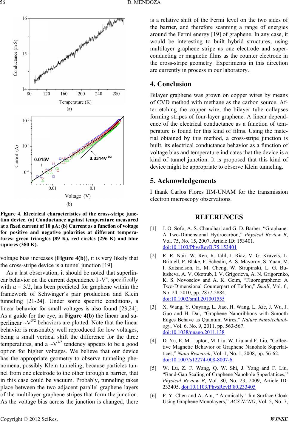 D. MENDOZA 56 (a) (b) Figure 4. Electrical characteristics of the cross-stripe junc- tion device. (a) Conductance against temperature measured at a fixed current of 10 μA; (b) Current as a function of voltage for positive and negative polarities at different tempera- tures: green triangles (89 K), red circles (296 K) and blue squares (380 K). voltage bias increases (Figure 4(b)), it is very likely that the cross-stripe device is a tunnel junction [19]. As a last observation, it should be noted that superlin- ear behavior on the current dependence I~Vα, specifically with α = 3/2, has been predicted for graphene within the framework of Schwinger´s pair production and Klein tunneling [21-24]. Under some specific conditions, a linear behavior for small voltages is also found [23,24]. As a guide for the eye, in Figure 4(b) the linear and su- perlinear ~V3/2 behaviors are plotted. Note that the linear behavior is reasonably well reproduced for low voltages, being a small vertical shift the difference for the three temperatures, and a ~V3/2 tendency appears to be a good option for higher voltages. We believe that our device has the appropriate geometry to observe tunneling phe- nomena, possibly Klein tunneling, because particles tun- nel from one electrode to the other through a barrier, that in this case could be vacuum. Probably, tunneling takes place between the two adjacent parallel graphene layers of the multilayer graphene stripes that form the junction. As the voltage bias across the junction is changed, there is a relative shift of the Fermi level on the two sides of the barrier, and therefore scanning a range of energies around the Fermi energy [19] of graphene. In any case, it would be interesting to built hybrid structures, using multilayer graphene stripe as one electrode and super- conducting or magnetic films as the counter electrode in the cross-stripe geometry. Experiments in this direction are currently in process in our laboratory. 4. Conclusion Bilayer graphene was grown on copper wires by means of CVD method with methane as the carbon source. Af- ter etching the copper wire, the bilayer tube collapses forming stripes of four-layer graphene. A linear depend- ence of the electrical conductance as a function of tem- perature is found for this kind of films. Using the mate- rial obtained by this method, a cross-stripe junction is built, its electrical conductance behavior as a function of voltage bias and temperature indicates that the device is a kind of tunnel junction. It is proposed that this kind of device might be appropriate to observe Klein tunneling. 5. Acknowledgements I thank Carlos Flores IIM-UNAM for the transmission electron microscopy observations. REFERENCES [1] J. O. Sofo, A. S. Chaudhari and G. D. Barber, “Graphane: A Two-Dimensional Hydrocarbon,” Physical Review B, Vol. 75, No. 15, 2007, Article ID: 153401. doi:10.1103/PhysRevB.75.153401 [2] R. R. Nair, W. Ren, R. Jalil, I. Riaz, V. G. Kravets, L. Britnell, P. Blake, F. Schedin, A. S. Mayorov, S. Yuan, M. I. Katsnelson, H. M. Cheng, W. Strupinski, L. G. Bu- lusheva, A. V. Okotrub, I. V. Grigorieva, A. N. Grigorenko, K. S. Novoselov and A. K. Geim, “Fluorographene: A Two-Dimensional Counterpart of Teflon,” Small, Vol. 6, No. 24, 2010, pp. 2877-2884. doi:10.1002/smll.201001555 [3] X. Wang, Y. Ouyang, L. Jiao, H. Wang, L. Xie, J. Wu, J. Guo and H. Dai, “Graphene Nanoribbons with Smooth Edges Behave as Quantum Wires,” Nature Nanotechnol- ogy, Vol. 6, No. 9, 2011, pp. 563-567. doi:10.1038/nnano.2011.138 [4] D. Yu, E. M. Lupton, M. Liu, W. Liu and F. Liu, “Collec- tive Magnetic Behavior of Graphene Nanohole Superlat- tices,” Nano Research, Vol. 1, No. 1, 2008, pp. 56-62. doi:10.1007/s12274-008-8007-6 [5] W. Lu, Z. F. Wang, Q. W. Shi, J. Yang and F. Liu, “Band-Gap Scaling of Graphene Nanohole Superlattices,” Physical Review B, Vol. 80, No. 23, 2009, Article ID: 233405. doi:10.1103/PhysRevB.80.233405 [6] P. Y. Chen and A. Alu, “ Atomically Thin Surface Cloak Using Graphene Monolayers,” ACS NANO, Vol. 5, No. 7, Copyright © 2012 SciRes. WJNSE  D. MENDOZA Copyright © 2012 SciRes. WJNSE 57 2011, pp. 5855-5863. doi:10.1021/nn201622e [7] A. Vakil and N. Engheta, “Transformation Optics Using Graphene,” Science, Vol. 332, No. 6035, 2011, pp. 1291- 1294. doi:10.1126/science.1202691 [8] G. Gao, T. Cagin and W. A. Goddard, “Energetics, Struc- ture, Mechanical and Vibrational Properties of Single- Walled Carbon Nanotubes,” Nanotechnology, Vol. 9, No. 3, 1998, pp. 184-191. doi:10.1088/0957-4484/9/3/007 [9] P. E. Lamert, P. Zhang and V. H. Crespi, “Gapping by Squashing: Metal-Insulator and Insulator-Metal Transi- tions in Collapsed Carbon Nanotubes,” Physical Review Letters, Vol. 84, No. 11, 2000, pp. 2453-2456. doi:10.1103/PhysRevLett.84.2453 [10] X. Li, W. Cai, J. An, S. Kim, J. Nah, D. Yang, R. Piner, A. Velamakanni, I. Jung, E. Tutu, S. K. Banerjee, L. Co- lombo and R. S. Ruoff, “Large-Area Synthesis of High- Quality and Uniform Graphene Films on Copper Foils,” Science, Vol. 324, No. 5932, 2009, pp. 1312-1314. doi:10.1126/science.1171245 [11] A. W. Robertson and J. H. Warner, “Hexagonal Single Crystal Domains of Few-Layer Graphene on Copper Foils,” Nano Letters, Vol. 11, No. 3, 2011, pp. 1182-1189. doi:10.1021/nl104142k [12] R. Wang, Y. Hao, Z. Wang, H. Gong and J. T. L. Thong, “Large-Diameter Graphene Nanotubes Synthesized Using Ni Nanowire Templates,” Nano Letters, Vol. 10, No. 12, 2010, pp. 4844-4850. doi:10.1021/nl102445x [13] C. Bautista and D. Mendoza, “Multilayer Graphene Syn- thesized by CVD Using Liquid Hexane as the Carbon Pre- cursor,” World Journal of Condensed Matter Physics, Vol. 1, No. 4, 2011, pp. 157-160. doi:10.4236/wjcmp.2011.14023 [14] R. R. Nair, P. Blake, A. N. Grigorenko, K. S. Novoselov, T. J. Booth, T. Stauber, N. M. R. Peres and A. K. Geim, “Fine Structure Constant Defines Visual Transparency of Graphene,” Science, Vol. 320, No. 5881, 2008, p. 1308. doi:10.1126/science.1156965 [15] S. Chen, W. Cai, R. D. Piner, J. W. Suk, Y. Wu, Y. Ren, J. Kang and R. S. Ruoff, “Synthesis and Characterization of Large-Area Graphene and Graphite Films on Commercial Cu-Ni Alloy Foils,” Nano Letters, Vol. 11, No. 9, 2011, pp. 3519-3525. doi:10.1021/nl201699j [16] M. Müller, M. Bräuninger and B. Trauzettel, “Tempera- ture Dependence of the Conductivity of Ballistic Gra- phene,” Physical Review Letters, Vol. 103, No. 19, 2009, Article ID: 196801. doi:10.1103/PhysRevLett.103.196801 [17] S. Adam and M. D. Stiles, “Temperature Dependence of the Diffusive Conductivity of Bilayer Graphene,” Physi- cal Review B, Vol. 82, No. 7, 2010, Article ID: 075423. doi:10.1103/PhysRevB.82.075423 [18] P. R. Wallace, “The Band Theory of Graphite,” Physical Review, Vol. 71, No. 9, 1947, pp. 622-634. doi:10.1103/PhysRev.71.622 [19] E. L. Wolf, “Principles of Electron Tunneling Spectros- copy,” Oxford University Press, New York, 1989. [20] M. S. Dresselhaus and G. Dresselhaus, “Intercalation Compounds of Graphite,” Advances in Physics, Vol. 30, No. 2, 1981, pp. 139-326. doi:10.1080/00018738100101367 [21] D. Allor, T. D. Cohen and D. A. McGady, “Schwinger Mechanism and Graphene,” Physical Review D, Vol. 78, No. 9, 2008, Article ID: 096009. doi:10.1103/PhysRevD.78.096009 [22] R. Rosenstein, M. Lewkowicz, H. C. Kao and Y. Korni- yenko, “Ballistic Transport in Graphene Beyond Linear Response,” Physical Review B, Vol. 81, No. 4, 2010, Ar- ticle ID: 041416. doi:10.1103/PhysRevB.81.041416 [23] B. Dóra and R. Moessner, “Nonlinear Electric Transport in Graphene: Quantum Quench Dynamics and the Schwinger Mechanism,” Physical Review B, Vol. 81, No. 16, 2010, Article ID: 165431. doi:10.1103/PhysRevB.81.165431 [24] N. Vandecastle, A. Barreiro, M. Lazzeri, A. Bachtold and F. Mauri, “Current-Voltage Characteristics of Graphene Devices: Interplay between Zenner-Klein Tunneling and Defects,” Physical Review B, Vol. 82, No. 4, 2010, Arti- cle ID: 045416. doi:10.1103/PhysRevB.82.045416 |