

Paper Menu >>
Journal Menu >>
 World Journal of Nano Science and Engineering, 2012, 2, 1-5 http://dx.doi.org/10.4236/wjnse.2012.21001 Published Online March 2012 (http://www.SciRP.org/journal/wjnse) 1 New Numerical Method to Calculate the True Optical Absorption of Hydrogen ated Nanocrystalline Silicon Thin Films Fatiha Besahraoui, Larbi Chahed, Yahia Bouizem, Jamal Dine Sib Laboratory of Physics of Thin Films and Materials for Electronics, University of Oran Es-Senia, Oran, Algeria Email: [email protected], {larbi.chahed, yahia.bouizem, jamaldine.sib}@univ-oran.dz Received November 14, 2011; revised December 18, 2011; accepted January 12, 2012 ABSTRACT The enhanced optical absorption measured by Constant Photocurrent Method (CPM) of hydrogenated nanocrystalline silicon thin films is due mainly to bulk and/or surface light scattering effects. A new numerical method is presented to calculate both true optical absorption and scattering coefficient from CPM absorption spectra of nanotextured nano- crystalline silicon films. Bulk and surface light scattering contributions can be unified through the correlation obtained between the scattering coefficient and surface roughness obtained using our method. Keywords: Solution Hydrogenated Nanocrystalline Silicon; Constant Photocurrent Method; Optical Absorption; Bulk Light Scattering; Surface Roughness; Film Thickness 1. Introduction Materials with nanometer crystallites constitute an im- portant class with some of their properties distinctly dif- ferent from either amorphous or large grain materials or single crystals. Especially, hydrogenated nanocrystalline and polymorphous silicon thin films. Hydrogenated nano- crystalline silicon (nano-Si:H) is an heterogeneous mate- rial. It consists of an ordered nanocrystallites of spherical form with size varies from 2 to 100 nm embedded in amorphous matrix [1]. These semiconducting nanomate- rials are very promising to the photovoltaic applications [2]. The important key for the success of nano-Si:H films as a PV absorbent materials is their enhanced absorption compared to the monocrystalline silicon (c Si), mainly in infrared region [3]. The main reason of this optical be- havior is due to their particular structure which gives place to the bulk and/or surface light scattering phenom- ena [3-5]. The Constant Photocurrent Method measure- ments of these heterogeneous mediums give us an “ap- parent” optical absorption coefficient at en- ergy E. is affected by light scattering effects different from true app E app E measured for homogeneous medi- ums, i.e., amorphous or monocrystalline silicon [3]. In this paper, we suggest a new numerical method to calcu- late the true optical absorption. A numerical resolution of Equation (1) is given at energy E = 1.1 eV. The contribu- tion of bulk light scattering, from the spectral depend- ence of apparent optical absorption coefficient app E in thin films of nano-Si:H is measured by Constant Photocurrent Method (CPM). The details of CPM method and its experimental configuration are described else- where [6]. This method is developed in order to under- stand the subgap part of the true optical absorption spec- tra related to the defect states within the energy gap. It’s introduced with the help of a recent theory [3] which describes the different contributions of light scattering in terms of photocurrent P h I deduced from CPM meas- urements. This procedure has a crucial importance to determine true in the case of weak bulk light scattering, without need to compare a several CPM measurements (for different interelectrodes spacing) [3]. We will pre- sent the details of our procedure and discuss its validity by comparing a calculated spectrum with the experimental one obtained by CPM for the same sample of nano-Si:H. Finally, we will apply this method on a series of nano-Si:H which have a different surface rough- ness in order to determine the correlation between this material parameter and the scattering coefficient true E s c . 2. Numerical Method In the following, let us consider a nano-Si:H thin film with a typical thickness df configured according to the CPM setup. If the standard CPM evaluation method will be applied to the measured spectrum, we will obtain an “apparent” optical absorption coefficient app fhich the following equation is valid [3]: or w C opyright © 2012 SciRes. WJNSE 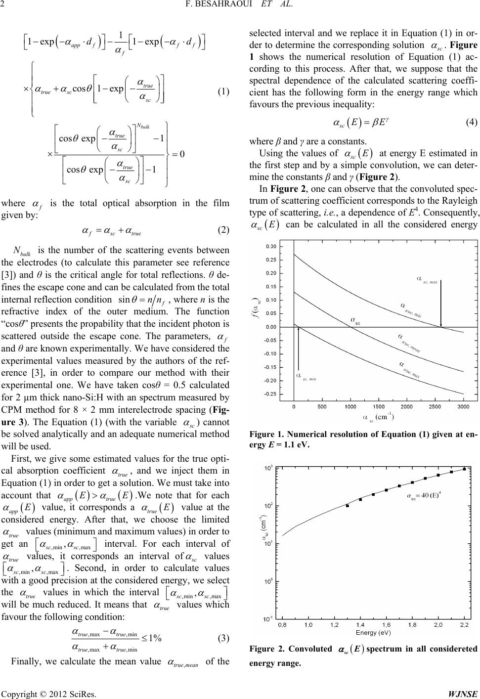 F. BESAHRAOUI ET AL. 2 1 1exp 1exp cos1 exp cos exp1 0 cos exp1 bulk app fff f true true sc sc N true sc true sc d d (1) where f is the total optical absorption in the film given by: f sc true (2) bulk is the number of the scattering events between the electrodes (to calculate this parameter see reference [3]) and θ is the critical angle for total reflections. θ de- fines the escape cone and can be calculated from the total internal reflection condition N sin f nn , where n is the refractive index of the outer medium. The function “cosθ” presents the propability that the incident photon is scattered outside the escape cone. The parameters, f and θ are known experimentally. We have considered the experimental values measured by the authors of the ref- erence [3], in order to compare our method with their experimental one. We have taken cosθ = 0.5 calculated for 2 µm thick nano-Si:H with an spectrum measured by CPM method for 8 × 2 mm interelectrode spacing (Fig- ure 3). The Equation (1) (with the variable s c ) cannot be solved analytically and an adequate numerical method will be used. First, we give some estimated values for the true opti- cal absorption coefficient true , and we inject them in Equation (1) in order to get a solution. We must take into account that E apptrue .We note that for each value, it corresponds a value at the considered energy. After that, we choose the limited true E true E app E values (minimum and maximum values) in order to get an ,min,maxsc sc interval. For each interval of , true values, it corresponds an interval of s c values ,min ,max . Second, in order to calculate values with a good precision at the considered energy, we select the true , sc sc values in which the interval ,min ,maxscsc will be much reduced. It means that , true values which favour the following condition: ,max,min ,max,min 1% true true true true (3) Finally, we calculate the mean value ,true mean of the selected interval and we replace it in Equation (1) in or- der to determine the corresponding solution s c . Figure 1 shows the numerical resolution of Equation (1) ac- cording to this process. After that, we suppose that the spectral dependence of the calculated scattering coeffi- cient has the following form in the energy range which favours the previous inequality: sc EE (4) where β and γ are a constants. Using the values of sc E at energy E estimated in the first step and by a simple convolution, we can deter- mine the constants β and γ (Figure 2). In Figure 2, one can observe that the convoluted spec- trum of scattering coefficient corresponds to the Rayleigh type of scattering, i.e., a dependence of E4. Consequently, sc E can be calculated in all the considered energy Figure 1. Numerical resolution of Equation (1) given at en- ergy E = 1.1 eV. Figure 2. Convoluted sc E spectrum in all considereted energy rang e. Copyright © 2012 SciRes. WJNSE 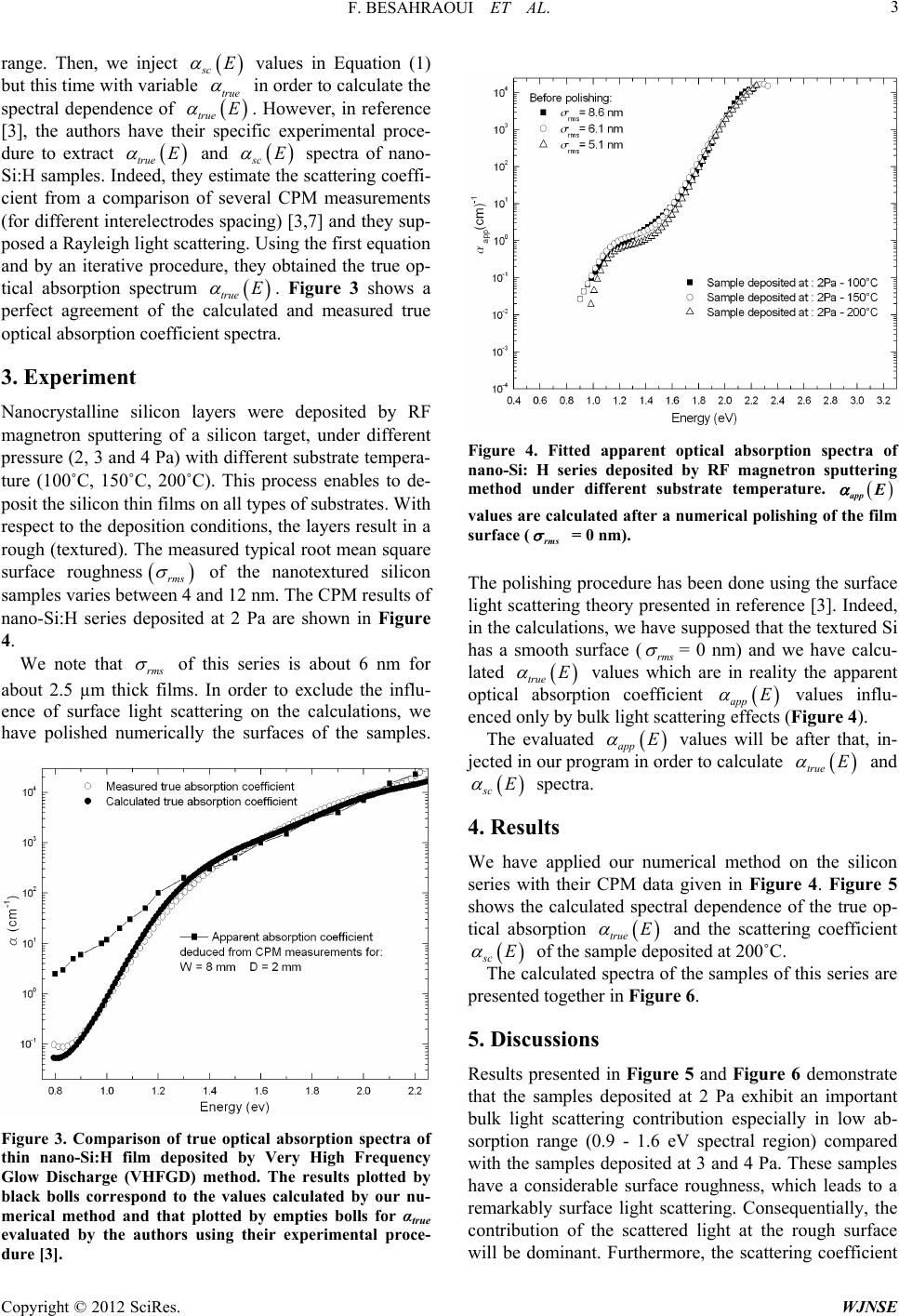 F. BESAHRAOUI ET AL. 3 range. Then, we inject values in Equation (1) but this time with variable sc E true in order to calculate the spectral dependence of . However, in reference [3], the authors have their specific experimental proce- dure to extract true and spectra of nano- Si:H samples. Indeed, they estimate the scattering coeffi- cient from a comparison of several CPM measurements (for different interelectrodes spacing) [3,7] and they sup- posed a Rayleigh light scattering. Using the first equation and by an iterative procedure, they obtained the true op- tical absorption spectrum . Figure 3 shows a perfect agreement of the calculated and measured true optical absorption coefficient spectra. true E sc true E E E 3. Experiment Nanocrystalline silicon layers were deposited by RF magnetron sputtering of a silicon target, under different pressure (2, 3 and 4 Pa) with different substrate tempera- ture (100˚C, 150˚C, 200˚C). This process enables to de- posit the silicon thin films on all types of substrates. With respect to the deposition conditions, the layers result in a rough (textured). The measured typical root mean square surface roughness of the nanotextured silicon samples varies between 4 and 12 nm. The CPM results of nano-Si:H series deposited at 2 Pa are shown in Figure 4. rms We note that rms of this series is about 6 nm for about 2.5 µm thick films. In order to exclude the influ- ence of surface light scattering on the calculations, we have polished numerically the surfaces of the samples. Figure 3. Comparison of true optical absorption spectra of thin nano-Si:H film deposited by Very High Frequency Glow Discharge (VHFGD) method. The results plotted by black bolls correspond to the values calculated by our nu- merical method and that plotted by empties bolls for αtrue evaluated by the authors using their experimental proce- dure [3]. Figure 4. Fitted apparent optical absorption spectra of nano-Si: H series deposited by RF magnetron sputtering method under different substrate temperature. app E values are calculated after a numerical polishing of the film surface ( rms = 0 nm). The polishing procedure has been done using the surface light scattering theory presented in reference [3]. Indeed, in the calculations, we have supposed that the textured Si has a smooth surface (rms = 0 nm) and we have calcu- lated true E values which are in reality the apparent optical absorption coefficient app E values influ- enced only by bulk light scattering effects (Figure 4). The evaluated app E values will be after that, in- jected in our program in order to calculate true E and sc E spectra. 4. Results We have applied our numerical method on the silicon series with their CPM data given in Figure 4. Figure 5 shows the calculated spectral dependence of the true op- tical absorption true E and the scattering coefficient sc E of the sample deposited at 200˚C. The calculated spectra of the samples of this series are presented together in Figure 6. 5. Discussions Results presented in Figure 5 and Figure 6 demonstrate that the samples deposited at 2 Pa exhibit an important bulk light scattering contribution especially in low ab- sorption range (0.9 - 1.6 eV spectral region) compared with the samples deposited at 3 and 4 Pa. These samples have a considerable surface roughness, which leads to a remarkably surface light scattering. Consequentially, the contribution of the scattered light at the rough surface will be dominant. Furthermore, the scattering coefficient Copyright © 2012 SciRes. WJNSE 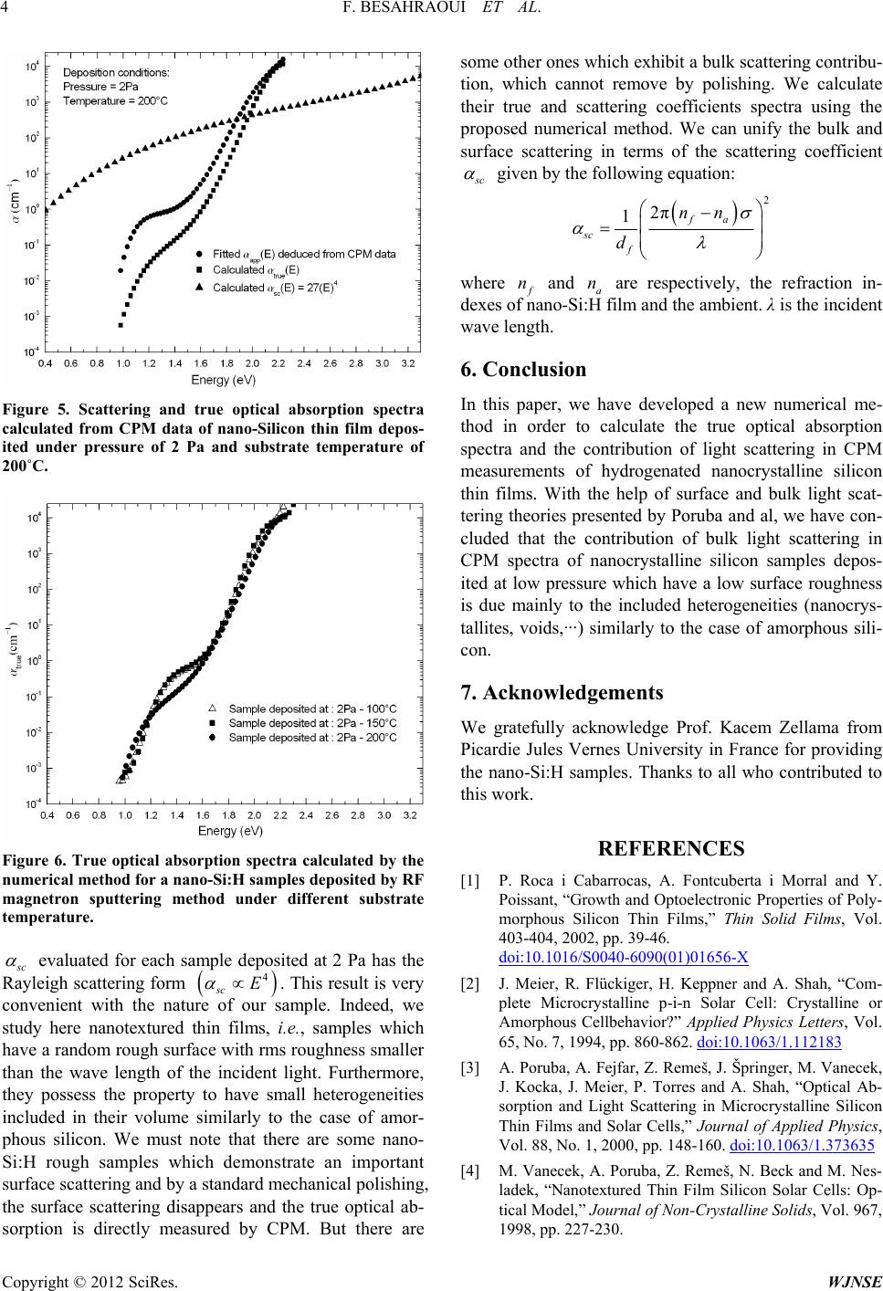 F. BESAHRAOUI ET AL. 4 Figure 5. Scattering and true optical absorption spectra calculated from CPM data of nano-Silicon thin film depos- ited under pressure of 2 Pa and substrate temperature of 200˚C. Figure 6. True optical absorption spectra calculated by the numerical method for a nano-Si:H samples deposite d by RF magnetron sputtering method under different substrate temperature. s c evaluated for each sample deposited at 2 Pa has the Rayleigh scattering form . This result is very convenient with the nature of our sample. Indeed, we study here nanotextured thin films, i.e., samples which have a random rough surface with rms roughness smaller than the wave length of the incident light. Furthermore, they possess the property to have small heterogeneities included in their volume similarly to the case of amor- phous silicon. We must note that there are some nano- Si:H rough samples which demonstrate an important surface scattering and by a standard mechanical polishing, the surface scattering disappears and the true optical ab- sorption is directly measured by CPM. But there are 4 sc E some other ones which exhibit a bulk scattering contribu- tion, which cannot remove by polishing. We calculate their true and scattering coefficients spectra using the proposed numerical method. We can unify the bulk and surface scattering in terms of the scattering coefficient s c given by the following equation: 2 2π 1fa nn sc f d where f n n and a are respectively, the refraction in- dexes of nano-Si:H film and the ambient. λ is the incident wave length. 6. Conclusion In this paper, we have developed a new numerical me- thod in order to calculate the true optical absorption spectra and the contribution of light scattering in CPM measurements of hydrogenated nanocrystalline silicon thin films. With the help of surface and bulk light scat- tering theories presented by Poruba and al, we have con- cluded that the contribution of bulk light scattering in CPM spectra of nanocrystalline silicon samples depos- ited at low pressure which have a low surface roughness is due mainly to the included heterogeneities (nanocrys- tallites, voids,...) similarly to the case of amorphous sili- con. 7. Acknowledgements We gratefully acknowledge Prof. Kacem Zellama from Picardie Jules Vernes University in France for providing the nano-Si:H samples. Thanks to all who contributed to this work. REFERENCES [1] P. Roca i Cabarrocas, A. Fontcuberta i Morral and Y. Poissant, “Growth and Optoelectronic Properties of Poly- morphous Silicon Thin Films,” Thin Solid Films, Vol. 403-404, 2002, pp. 39-46. doi:10.1016/S0040-6090(01)01656-X [2] J. Meier, R. Flückiger, H. Keppner and A. Shah, “Com- plete Microcrystalline p-i-n Solar Cell: Crystalline or Amorphous Cellbehavior?” Applied Physics Letters, Vol. 65, No. 7, 1994, pp. 860-862. doi:10.1063/1.112183 [3] A. Poruba, A. Fejfar, Z. Remeš, J. Špringer, M. Vanecek, J. Kocka, J. Meier, P. Torres and A. Shah, “Optical Ab- sorption and Light Scattering in Microcrystalline Silicon Thin Films and Solar Cells,” Journal of Applied Physics, Vol. 88, No. 1, 2000, pp. 148-160. doi:10.1063/1.373635 [4] M. Vanecek, A. Poruba, Z. Remeš, N. Beck and M. Nes- ladek, “Nanotextured Thin Film Silicon Solar Cells: Op- tical Model,” Journal of Non-Crystalline Solids, Vol. 967, 1998, pp. 227-230. Copyright © 2012 SciRes. WJNSE  F. BESAHRAOUI ET AL. Copyright © 2012 SciRes. WJNSE 5 [5] A. Poruba, Z. Remeš, J. Špringer, M. Vanecek, A. Fejfar, J. Kocka, J. Meier, P. Torres and A. Shah, “Light Scat- tering in Microcrystalline Thin Film Cells,” Proceeding of the 2nd World Conference & Exhibition on Photo- voltaic Energy Conversion, Vienna, July 1998, pp. 781- 784. [6] M. Vanecek, J. Kocka, A. Poruba and A. Fejfar, “Direct Measurement of the Deep Defect Density in Thin Amor- phous Silicon Films with the Absolute Constant Photo- current Method,” Journal of Applied Physics, Vol. 78, No. 10, 1995, pp. 6203-6210. doi:10.1063/1.360566 [7] M. Vanecek, J. Houloubek and A. Shah, “Optical Study of Microvoids, Voids, and Local Inhomogeneities in Amor- phous Silicon,” Applied Physics Letters, Vol. 59, No. 18, 1991, pp. 2237-2239. doi:10.1063/1.106081 |