

Paper Menu >>
Journal Menu >>
 Journal of Crystallization Process and Technology, 2012, 2, 12-15 http://dx.doi.org/10.4236/jcpt.2012.21002 Published Online January 2012 (http://www.SciRP.org/journal/jcpt) Analysis of μ-Czochralski Technique Using Two-Dimensional Crystallization Simulator Kuniaki Matsuki1, Ryusuke Saito1, Shuji Tsukamoto1, Mutsumi Kimura1,2, Ryoichi Ishihara3 1Department of Electronics and Informatics, Ryukoku University, Otsu, Japan; 2Joint Research Center for Science and Technology, Ryukoku University, Otsu, Japan; 3Delft Institute of Microelectronics and Submicrontechnology, Delft University of Technology, Delft, Netherlands. Email: [email protected] Received December 4th, 2011; revised January 5th, 2012; accepted January 16th, 2012 ABSTRACT -Czochralski technique has been analyzed using two-dimensional crystallization simulator. It is observed that the temperature is relatively uniform in the entire Si region after the laser irradiation because the heat conductivity of the Si region is much higher than that of the underneath SiO2. Grain growth advances from the grain filter to the channel re- gion and continues until it collides with what advances from random nucleation in the channel region. When the initial temperature is high, the random nucleation rarely occurs even under the supercooling condition, and the grain size be- comes large. Moreover, it is qualitatively reproduced that the grain size increases as the irradiated energy of the laser irradiation increases. Keywords: -Czochralski Technique; Two Dimensional Crystallization Simulator; Grain Growth; Grain Filter; Grain Size 1. Introduction -Czochralski technique is a crystallization technique to enlarge poly-Si grains in thin-film transistors (TFTs) not only for flat panel displays and but also for general elec- tronics [1,2]. In the -Czochralski technique, grain filters are bored in underneath SiO2 films, amorphous-Si films are deposited and filled into the grain filters, excimer laser are irradiated to the amorphous-Si films, and grain growth advances from the grain filter and to the channel regions. Although the -Czochralski technique has been experi- mentally analyzed in detail [3-6], the crystallization pro- cess should be theoretically clarified. Recently, a two-dimensional (2-D) crystallization simu- lator has been developed and proposed as a practical eva- luation tool for poly-Si TFTs [7]. In the 2-D crystallization simulator, random nucleation, crystal growth velocity, la- tent heat emission, and partial crystallization are modeled. In this paper, we analyze the -Czochralski technique using the 2-D crystallization simulator. We evaluate the temperature, grain growth, nucleation, etc. We try to repro- duce the dependence of the grain size on the irradiated energy of the laser irradiation. 2. 2-D Crystallization Simulator The 2-D crystallization simulator is minutely explained in a previous paper [7]. Roughly speaking, the nucleation rate is defined as a function of temperature following a classical nucleation theory, and the crystal growth veloc- ity is also defined as a function of temperature following a classical crystal growth theory. The partial crystalliza- tion model is used allowing the co-existence of the liquid and crystal phases even in a finite element. The simulation algorithm is composed of the phase transition and heat transfer algorithms. The thermal properties of Si and SiO2 are listed in the previous paper. The grain filters are located in underneath SiO2 films, and grain seeds are put at the bottoms of the grain filters. The depth and diameter of the grain filters are 250 nm and 50 nm. The grain seeds consist of fine grains formed dur- ing explosive crystallization at the beginning of the laser irradiation [3]. The channel regions are melt to the liquid- Si, and initial temperature of the liquid-Si is varied. The thickness of the channel regions is 250 nm. The nuclea- tion, grain growth, and temperature are successively cal- culated with the time after the laser irradiation. The cal- culation area is more than 2.5 m. It should be noted that the initial temperature is set instead of giving the irradi- ated energy of the laser irradiation. The initial tempera- ture is not the temperature at the laser irradiation, but the temperature at the start of the crystallization simulation. 3. Simulation Results The distribution of the temperature in the grain filter, Copyright © 2012 SciRes. JCPT 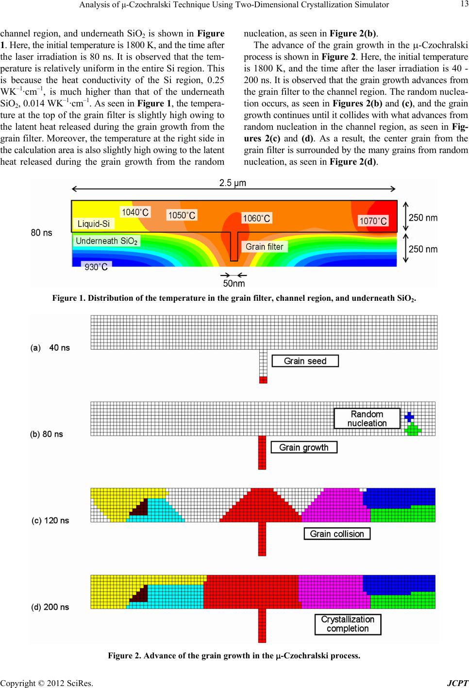 Analysis of μ-Czochralski Technique Using Two-Dimensional Crystallization Simulator 13 channel region, and underneath SiO2 is shown in Figure 1. Here, the initial temperature is 1800 K, and the time after the laser irradiation is 80 ns. It is observed that the tem- perature is relatively uniform in the entire Si region. This is because the heat conductivity of the Si region, 0.25 WK–1·cm–1, is much higher than that of the underneath SiO2, 0.014 WK–1·cm–1. As seen in Figure 1, the tempera- ture at the top of the grain filter is slightly high owing to the latent heat released during the grain growth from the grain filter. Moreover, the temperature at the right side in the calculation area is also slightly high owing to the latent heat released during the grain growth from the random nucleation, as seen in Figure 2(b). The advance of the grain growth in the -Czochralski process is shown in Figure 2. Here, the initial temperature is 1800 K, and the time after the laser irradiation is 40 - 200 ns. It is observed that the grain growth advances from the grain filter to the channel region. The random nuclea- tion occurs, as seen in Figures 2(b) and (c), and the grain growth continues until it collides with what advances from random nucleation in the channel region, as seen in Fig- ures 2(c) and (d). As a result, the center grain from the grain filter is surrounded by the many grains from random nucleation, as seen in Figure 2(d). Figure 1. Distribution of the temperature in the grain filter, channel region, and underneath SiO2. Figure 2. Advance of the grain growth in the -Czochralski process. Copyright © 2012 SciRes. JCPT 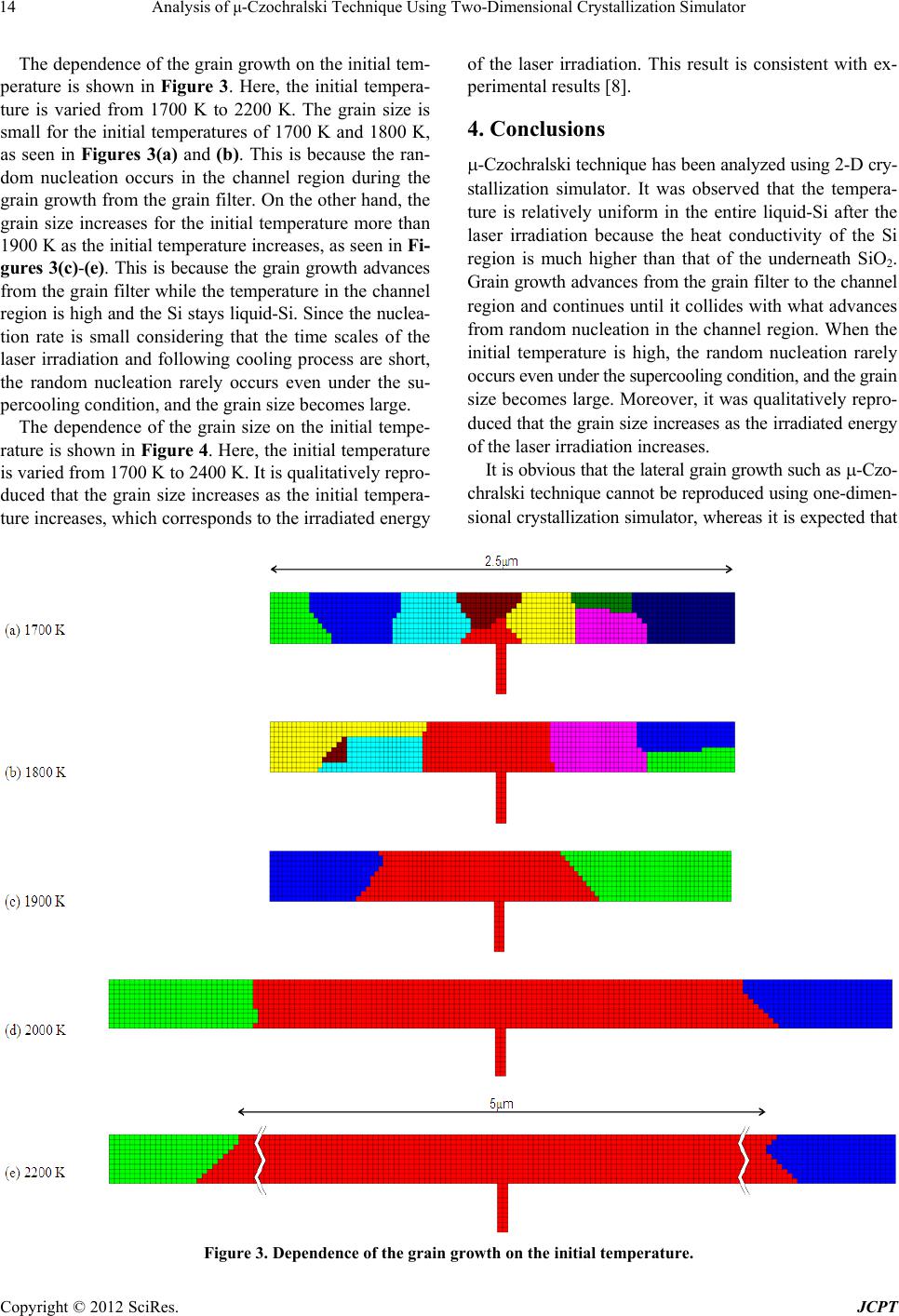 Analysis of μ-Czochralski Technique Using Two-Dimensional Crystallization Simulator 14 The dependence of the grain growth on the initial tem- perature is shown in Figure 3. Here, the initial tempera- ture is varied from 1700 K to 2200 K. The grain size is small for the initial temperatures of 1700 K and 1800 K, as seen in Figures 3(a) and (b). This is because the ran- dom nucleation occurs in the channel region during the grain growth from the grain filter. On the other hand, the grain size increases for the initial temperature more than 1900 K as the initial temperature increases, as seen in Fi- gures 3(c)-(e). This is because the grain growth advances from the grain filter while the temperature in the channel region is high and the Si stays liquid-Si. Since the nuclea- tion rate is small considering that the time scales of the laser irradiation and following cooling process are short, the random nucleation rarely occurs even under the su- percooling condition, and the grain size becomes large. The dependence of the grain size on the initial tempe- rature is shown in Figure 4. Here, the initial temperature is varied from 1700 K to 2400 K. It is qualitatively repro- duced that the grain size increases as the initial tempera- ture increases, which corresponds to the irradiated energy of the laser irradiation. This result is consistent with ex- perimental results [8]. 4. Conclusions -Czochralski technique has been analyzed using 2-D cry- stallization simulator. It was observed that the tempera- ture is relatively uniform in the entire liquid-Si after the laser irradiation because the heat conductivity of the Si region is much higher than that of the underneath SiO2. Grain growth advances from the grain filter to the channel region and continues until it collides with what advances from random nucleation in the channel region. When the initial temperature is high, the random nucleation rarely occurs even under the supercooling condition, and the grain size becomes large. Moreover, it was qualitatively repro- duced that the grain size increases as the irradiated energy of the laser irradiation increases. It is obvious that the lateral grain growth such as -Czo- chralski technique cannot be reproduced using one-dimen- sional crystallization simulator, whereas it is expected that Figure 3. Dependence of the grain growth on the initial temperature. Copyright © 2012 SciRes. JCPT 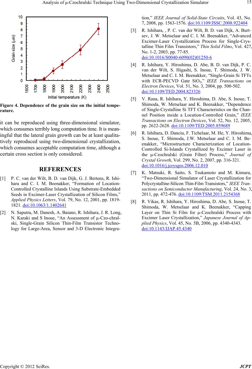 Analysis of μ-Czochralski Technique Using Two-Dimensional Crystallization Simulator 15 Figure 4. Dependence of the grain size on the initial tempe- rature. it can be reproduced using three-dimensional simulator, which consumes terribly long computation time. It is mean- ingful that the lateral grain growth can be at least qualita- tively reproduced using two-dimensional crystallization, which consumes acceptable computation time, although a certain cross section is only considered. REFERENCES [1] P. C. van der Wilt, B. D. van Dijk, G. J. Bertens, R. Ishi- hara and C. I. M. Beenakker, “Formation of Location- Controlled Crystalline Islands Using Substrate-Embedded Seeds in Excimer-Laser Crystallization of Silicon Films,” Applied Physics Letters, Vol. 79, No. 12, 2001, pp. 1819- 1821. doi:10.1063/1.1402641 [2] N. Saputra, M. Danesh, A. Baiano, R. Ishihara, J. R. Long, N. Karaki and S Inoue, “An Assessment of µ-Czo-chral- ski, Single-Grain Silicon Thin-Film Transistor Techno- logy for Large-Area, Sensor and 3-D Electronic Integra- tion,” IEEE Journal of Solid-State Circuits, Vol. 43, No. 7, 2008, pp. 1563-1576. doi:10.1109/JSSC.2008.922404 [3] R. Ishihara, , P. C. van der Wilt, B. D. van Dijk, A. Burt- sev, J. W. Metselaar and C. I. M. Beenakker, “Advanced Excimer-Laser Crystallization Process for Single-Crys- talline Thin Film Transistors,” Thin Solid Films, Vol. 427, No. 1-2, 2003, pp. 77-85. doi:10.1016/S0040-6090(02)01250-6 [4] R. Ishihara, Y. Hiroshima, D. Abe, B. D. van Dijk, P. C. van der Wilt, S. Higashi, S. Inoue, T. Shimoda, J. W. Metselaar and C. I. M. Beenakker, “Single-Grain Si TFTs with ECR-PECVD Gate SiO2,” IEEE Transactions on Electron Devi ces, Vol. 51, No. 3, 2004, pp. 500-502. doi:10.1109/TED.2004.823326 [5] V. Rana, R. Ishihara, Y. Hiroshima, D. Abe, S. Inoue, T. Shimoda, W. Metselaar and K. Beenakker, “Dependence of Single-Crystalline Si TFT Characteristics on the Chan- nel Position inside a Location-Controlled Grain,” IEEE Transactions on Electron Devices, Vol. 52, No. 12, 2005, pp. 2622-2628. doi:10.1109/TED.2005.859689 [6] R. Ishihara, D. Danciu, F. Tichelaar, M. He, Y. Hiroshima, S. Inoue, T. Shimoda, J.W. Metselaar and C. I. M. Be- enakker, “Microstructure Characterization of Location- Controlled Si-Islands Crystallized by Excimer Laser in the μ-Czochralski (Grain Filter) Process,” Journal of Crystal Growth, Vol. 299, No. 2, 2007, pp. 316-321. doi:10.1016/j.jcrysgro.2006.12.010 [7] K. Matsuki, R. Saito, S. Tsukamoto and M. Kimura, “Two-Dimensional Simulator of Laser Crystallization for Polycrystalline-Silicon Thin-Film Transistors,” IEE E Tran- sactions on Semiconductor Manufacturing, Vol. 24, No. 3, 2011, pp. 472-476. doi:10.1109/TSM.2011.2154368 [8] R. Vikas, R. Ishihara, Y. Hiroshima, D. Abe, S. Inoue, T. Shimoda, W. Metselaar and K. Beenakker, “Capping Layer on Thin Si Film for µ-Czochralski Process with Excimer Laser Crystallization,” Japanese Journal of Ap- plied Physics, Vol. 45, No. 5B, 2006, pp. 4340-4343. doi:10.1143/JJAP.45.4340 Copyright © 2012 SciRes. JCPT |